CTSD Precision ADCs (Part 4): Ease of ADC Input and Reference Drive Simplify Signal-Chain Design
This article is part of the Analog Series: Optimizing Digital Processing with CTSD Precision ADCs
Members can download this article in PDF format.
What you'll learn:
- A look at the design of traditional ADC front ends.
- How to simplify the input drive of CTSD ADCs.
- Simplifying reference and reference-drive designs.
The key to achieving optimal signal chain performance is ensuring that the input source or the reference itself isn’t corrupted when interfaced with an analog-to-digital converter (ADC). With traditional ADCs, complex signal-condition circuitry design, otherwise referred to as front-end design, is required for the seamless interface of input and reference to the ADC.
The unique architectural properties of continuous-time sigma-delta (CTSD) ADCs enable simplified and innovative ways of interfacing this ADC to the input and reference. To begin, let’s quickly recap traditional ADC front-end designs.
Front-End Design for Traditional ADCs
In this article, we will use the terms “sensor” or “input signal” interchangeably to represent any kind of voltage input to the ADC signal chain. The input signal for the ADC signal chain could be a sensor, a signal from some source, or the feedback of a control loop.
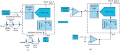
It’s well-known that in traditional discrete-time sigma-delta (DTSD) ADCs and successive-approximation-register (SAR) ADCs, the sampling network at the input and reference is a switched capacitor load. When the switch turns ON, the capacitor is charged to the input, and when it turns OFF, the capacitor holds the sampled value. At every sampling clock edge, when the switch reconnects the capacitor to the input, a finite current called “kickback current” is required to charge or discharge the capacitor to the new sampled value. The profile of the current is shown in Figure 1a.
Most sensors and reference ICs fall short of driving such magnitudes of kickback currents, and if directly interfaced to the ADC, there’s a high probability of the input signal or reference becoming corrupted. One of the known solutions to avoid this corruption is to use a driving buffer amplifier to isolate the input sensor and the reference from the ADC. The driver amplifier should be able to to absorb these kickback currents as shown in Figure 1b.
This leads to the requirement of a high slew rate and a high-bandwidth amplifier to support the required input charging/discharging currents and settle the kickbacks within one sampling time period. These stringent requirements limit the choice of buffer amplifiers that can be used on input and reference paths for the traditional ADCs.
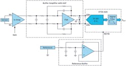
On the other hand, a low-pass antialiasing filter is required on the input to ensure high-frequency noise and interferers are heavily attenuated. Thus, when they fold back due to sampling into the frequency band of interest, performance isn’t degraded. The challenge for incumbent ADC signal-chain designers is to fine-tune the opposing requirements of alias rejection and output settling. The front-end design with driver and antialiasing filter for a DTSD ADC is shown in Figure 2.
The input path consists of an instrumentation amplifier (in-amp) that interfaces the sensor to a fully differential amplifier (FDA), which finally drives the ADC. The in-amp isolates the input sensor environment from the ADC circuit. For example, the common-mode (CM) signal of the sensor can be very high, up to tens of volts. But most FDAs and ADCs don’t support this high input common-mode voltage.
A general in-amp has the capability to support wide input common mode while providing an output common mode suitable for the FDA and ADC. Another advantage of an in-amp is that it has high input impedance. This means that if the sensor can’t drive the input resistor of the FDA directly, then the sensor can be interfaced with an FDA using an in-amp. The FDA itself would require a high bandwidth and slew rate for faster output settling. An active antialiasing filter (AAF) required for the interferer’s immunity is built around the FDA.
The drivers of the input or the reference have conflicting requirements: On the one hand, high bandwidth is desired for settling, but on the other, low bandwidth is required to filter noise and interferers. On the reference path, the front-end design for the DTSD ADC signal chain (Fig. 2, again) has a reference IC connected to a buffer that drives the reference load of the ADC. It also includes a noise filter that cuts off the noise of the reference IC and buffer beyond a certain frequency. The design requirements of this filter are discussed in a later section. The reference buffer has high bandwidth and slew-rate requirements for faster settling of the sampling event disturbances.
Part 1 of this series demonstrated that a new signal chain using a precision CTSD ADC could be 68% smaller than the complex signal chains of traditional ADCs. This size reduction decreases the BOM, and the simplicity helps signal-chain designers achieve faster time to market.
CTSD ADC Advantage: Resistive Input and Reference
In Part 2, the CTSD ADC architecture was explained to signal-chain designers with an unconventional approach to inverting closed-loop amplifiers. As noted in Part 2, a CTSD ADC can be envisioned as a sigma-delta ADC with a resistive input and reference load. The input and reference structure are a simple resistive load, which means there are no high bandwidth or high slew-rate drive requirements.
Part 3 demonstrated the unique advantages of a CTSD that offers interference immunity due to its inherent alias rejection. In a traditional signal-chain design, the external alias rejection filter needed to attenuate the interferers is an added challenge, while CTSD ADCs have no need for an external AAF.
Due to the inherent alias rejection property of CTSD ADCs, the signal-transfer function of the modulator loop equates to an antialiasing filter that attenuates the high-frequency interferers. Because of the resistive input and inherent AAF, the input network is simplified, and the sensor can be directly connected to the ADC.
In cases where sensors may not have the capability to drive such a resistive load, an in-amp could be used to interface the sensor to the ADC. Similarly, on the reference side, due to the resistive load, the reference buffer is eliminated in the CTSD ADC signal chain. Figure 3b shows a simplified schematic with an in-amp.
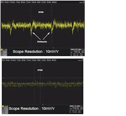
Figure 4 shows further support for how CTSD ADCs help simplify input front-end design. For the DTSD ADC, the discontinuities in input current caused by kickbacks when the input sampling switch changes state are noticeably seen. With the CTSD ADC, the input current is observed to be continuous, which maintains signal continuity.
The Simplified Input Drive Design
We’ve established that the input drive of the CTSD ADC is resistive. This section will address the value of the input impedance RIN in planning for the input drive of the ADC. RIN is a function of the noise performance specified for the ADC.
For example, in the AD4134, which is a precision CTSD ADC with a dynamic range of 108 dB with 4-V reference, the input impedance is 6-kΩ differential. This indicates that when a full-scale 8-V p-p differential input signal is applied to the ADC, the peak current requirement is 1.3 mA p-p. If the sensor can support the input current VIN/RIN, then it can be directly interfaced to the ADC.
The scenarios where a simple amplifier would be required to drive this resistive load are:
- When the sensor doesn’t have the drive capability to provide the peak current of VIN/RIN.
- Signal-chain design dictates that gain or attenuation is required for the sensor output.
- Isolating the input sensor environment from the ADC circuit.
- The sensor has a large output impedance.
- The sensor is far from the ADC and the track routing could add significant resistance to the input.
In scenarios 4 and 5, there would be a voltage drop across the extra external resistor Rs, indicating a signal loss at the ADC input. This leads to gain errors for the signal chain and drift of errors with temperature, which can lead to performance degradation. The temperature gain drift is caused by the different temperature coefficients of the external resistance and internal resistance.
Such a problem can be solved with a simple amplifier to isolate the extra external resistance. Because the driving load for this amplifier is resistive, the selection criteria of this amplifier are:
- Input impedance: To avoid signal attenuation or loss, the impedance of the sensor should be matched with the amplifier input impedance.
- Output impedance: The output impedance should be sufficient to drive the resistive input load of the ADC.
- Output type: As a general signal-chain design guideline, a differential signaling strategy is recommended for best signal-chain performance. A differential-output-type amplifier or a design technique for single-ended to differential output is best suited for this task. Also, for the best performance, it’s preferable to set the common mode of this differential signal to VREF/2.
- Programmable gain: The input signal is generally gained or attenuated to map it to the full-scale range of the ADC. This is because the maximum performance can be obtained from an ADC signal chain when the full input range of its ADC is used.
Based on the application, this amplifier could be an in-amp, an FDA, or combination of two single-ended op amps forming a differential output amplifier. With no rigid requirements of high slew rate or high bandwidth, a wide range of amplifiers developed by ADI is available to drive this CTSD ADC based on application requirements. In addition, amplifier performance parameters are generally specified with a resistive load, which makes the selection more straightforward.
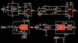
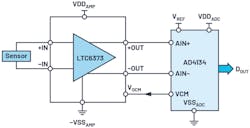
As an example, for the AD4134, one option for a performance-compatible in-amp with programmable gain options and fully differential outputs is the LTC6373. This in-amp provides high impedance to the input source and can drive the differential 6-kΩ impedance with noise and linearity performance on par with the ADC. With its wide range of input common-mode support and programmable gain options, any sensors or input signals with a wide range of signal magnitude can be interfaced with the ADC. Figure 5 shows an example of input front-end design with this direct in-amp drive.
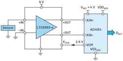
Another example is a low-voltage simple front-end design using a fully differential driver amplifier like the LTC6363-0.5/LTC6363-1/LTC6363-2, based on the gain or attenuation required (Fig. 6). FDAs could be used in scenarios where the sensor can drive the resistive load of the FDA but is a single-ended type or has a common mode that’s not supported by the ADC, or it requires small gain/attenuation in the signal chain.
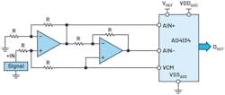
A further example includes a low-BOM option for single-ended input conversion to a fully differential signal at the ADC using two single-ended op amps (Fig. 7).
There are many other examples, like using a combination of a single-ended in-amp and single-ended op amp to build a differential output front end for a very-high-input CM or low-drive-strength single-ended type sensor. Any such combination can be selected based on performance, area, and BOM requirements to better suit the application.
Other amplifiers that are compatible with AD4134 include:
- Operational amplifiers: ADA4625-2, ADA4610-2, AD8605, and ADA4075-2
- Fully differential amplifiers: ADA4940-2, LTC6363, and ADA4945-1
- Instrumentation amplifier: AD8421
ADI’s amplifier selection guide can be used to select the best amplifier suited for an application. For example, the ADA4945-1 is recommended for high-linearity applications like audio test equipment. And in photodiode applications where the most important consideration is very high input impedance, a transimpedance amplifier (TIA) such as the ADA4610-2 can be used.
With the input front end dramatically simplified with a CTSD ADC, let’s have a look at the similar simplification of the reference drive.
The Simplified Reference Design
The ADC output is a representation of its input and reference, as given by Equation 1:
where VIN = input voltage level, VREFADC = reference of the ADC, N = number of bits, DOUT = ADC digital output.
Equation 1 indicates that, for the best ADC performance, a clean, uncorrupted reference is important. The three major performance metrics of the ADC signal chain affected by an error in the reference are:
Signal-to-noise ratio (SNR)
The major noise contributors to SNR are the input path, the ADC itself, and the reference. For a target total noise at the output of the ADC, accounting for the other noise contributors, the budget for the reference noise is generally 1/3 or 1/4 of standalone ADC output noise. The reference or reference buffers typically have higher noise than the ADC.
If we look at any datasheet for a reference or reference buffer IC, spectral noise density (or Noisedensity) is one of the specifications. If we revisit noise calculations basics, the total noise at the output of the reference or reference buffer is then given by:
We can’t control the Noisedensity as it’s fixed for the chosen reference or buffer. The only controllable parameter is the noise bandwidth (NBW). To target low reference noise, we reduce the noise bandwidth of the reference or reference buffer. This is generally done by connecting a first-order low-pass RC filter to the ADC (Fig. 8).
The ADC reference current, IADC, flowing through the filter resistor R causes a voltage drop, which changes the actual reference value at the ADC. Therefore, it is recommended to choose a small value of R and a large value of C to meet the NBW requirements for low reference noise.
Gain error
As is evident from Equation 1, VREFADC determines the slope of the output to input transfer function just like in a straight equation such as y = mx. This slope also is referred to as the gain of the ADC. Thus, if the reference changes, the gain of the ADC changes, too.
Linearity
For traditional DTSD ADCs and SAR ADCs, the reference current and the accompanying kickbacks depend on the input signal. Therefore, if the reference doesn’t settle completely before the next sampling clock edge, the error seen on the reference will be input dependent and cause nonlinearity. Mathematically, the VREFADC is then represented as:
Referring to Equation 1, the ADC output DOUT will have various higher-order dependencies based on the input of the ADC, and this dependency causes harmonics and integral nonlinearity. Hence, for traditional ADCs, there’s a hard requirement on the high slew rate and bandwidth of the reference buffer to settle the reference output within the sampling time period.
Addressing Reference Driver Challenges
If we carefully analyze the SNR and linearity, we see that the reference or reference buffer has quite conflicting requirements to satisfy. There’s a low bandwidth requirement for noise and a high bandwidth requirement for faster settling.
Tuning the fine balance between those two requirements has been an age-old challenge for signal-chain designers. Some of the latest DTSD ADCs and SAR ADCs have the reference buffer incorporated on-chip to ease one step in signal-chain design, but these solutions require additional power or come with certain performance penalties. Because CTSD ADCs don’t require a fast-settling buffer and have a resistive input to remove the need for a fast-settling driver, they’re able to avoid these performance problems.
The CTSD ADC addresses reference driver challenges with the following properties and design improvements:
- With the resistive load on reference, there’s no settling requirement at every sampling clock edge. As a result, designers can directly connect the reference IC to the ADC without needing a dedicated reference buffer.
- Patented design techniques make the reference current independent of the input and force the reference current of the ADC (IADC) to be substantially constant. This is beneficial when an RC filter may be required to reduce the reference noise (Fig. 8, again). The result is a constant voltage drop across the resistor with no input-dependent terms added to VREFADC. A provision is designed to digitally correct for the gain error at the system level depending on the value of R and the voltage measured at the reference pin. Hence, this simple reference interface will not have gain or linearity errors.
Even though a provision has been implemented to digitally correct for the error caused by the voltage drop across R, one might wonder if this would limit the full-scale range of the CTSD ADC, as the actual reference (VREFADC) of the ADC would be lesser than the applied VREF.
For example, if the VREF of the reference IC is trimmed and set to 4.096 V and the ADC reference current (IADC) = 6 mA, then, for a filter resistance of R = 20 Ω, the actual reference of the ADC (VREFADC) is 3.967 V. In such a case, when the specified full-scale differential input of 2 × VREF = 8.192 V p-p (which is greater than 2 × VREFADC) is applied at the input of the ADC, is there a possibility of saturating the output of the ADC? The answer is “no.”
CTSD ADCs are designed to support input magnitudes that are a few millivolts beyond the reference at the ADC pin, REFIN. In our example case of the AD4134, this extended range limits the resistor value to a maximum of 25 Ω. The value of C for the noise filter is then chosen to satisfy the noise bandwidth calculated.
Reference Drive Design Simplified
CTSD ADCs have eased the design of the reference drive, but additional factors still must be considered when selecting the correct R for the filter followed by digital gain error correction of the voltage drop across the resistor. Digital gain error correction, also known as calibration, is a common feature in many ADCs. It offers signal-chain designers the freedom to compensate for errors in the signal chain at the digital output of an ADC. As such, it may not require an added design step but rather reuse of the same algorithm, which is common for many signal chains.
At the face of it, then, the selection of resistor doesn’t seem to be a particularly involved design step, but there’s one caveat: the temperature dependence of the voltage drop. The external filter resistor and IADC drift differently with temperature, which in turn causes VREFADC and the gain of the ADC to drift with temperature. For applications with stringent gain drift requirements, a crude solution consists of calibrating the signal chain periodically.
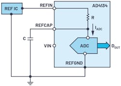
However, a much better and innovative solution is made possible thanks to CTSD technology. Since the ADC reference load current is a constant and function of resistive material used on-chip, it was possible to provide the filter resistor (R) with 20 Ω on-chip (Fig. 9).
In the new front-end design, the reference IC is connected at the REFIN pin and the filter capacitor is connected at the REFCAP pin to form the noise filter for the reference IC noise. Since the resistance of the on-chip resistor R and the IADC are both functions of the same resistor material, there’s no temperature drift on REFCAP (VREFADC). AD4134 also uses a patented on-chip reference correction algorithm to digitally self-calibrate for the voltage drop across the on-chip resistor. Thus, the reference drive design is now simplified to the selection of the reference IC and capacitor value based on the performance requirements.
ADR444 is one of the low-noise reference ICs that can be used as a companion for a CTSD ADC. The AD4134’s datasheet has further details on the capacitor value selection and the internal and external digital gain calibration.
Conclusion
CTSD ADCs eliminate many of the barriers to achieving optimal precision performance and simplified front-end design. In an upcoming article, we will cover how a CTSD ADC modulator core’s output is processed into its final digital output format for use by an external digital controller to optimize processing.
From the sigma-delta basics explained throughout this series, we know the modulator output can’t be processed directly because it’s sampled at a much higher rate. The sample rate must be reduced to the required output data rate (ODR) of the application.
In the upcoming Part 5, we will introduce a novel asynchronous sample-rate conversion (ASRC) technique. It enables signal-chain designers to tune the final ADC output at any desired ODR and go beyond the age-old restriction of limiting ODR to a multiple of sampling frequency.
Read more articles in the Analog Series: Optimizing Digital Processing with CTSD Precision ADCs
References
“Driving Precision Converters: Selecting Voltage References and Amplifiers.” Analog Devices, Inc.
Mahaffey, Anna. “Driving SAR ADCs Part 1: Analog Input Model.” Analog Devices, Inc.
Shah, Anshul. “Why Does Voltage Reference Noise Matter?” Analog Dialogue, Vol. 54, No. 1, March 2020.
