Single-Channel, High-Voltage Output DACs Include Precision Reference
In the broad-brush view of the analog-to-digital converter (ADC) versus its complement, the digital-to-analog converter (DAC), there’s no doubt that the DAC has an easier functional challenge.
What’s the difference? The ADC must capture an external, unknown, and random signal to translate it into its digital equivalent. In contrast, the DAC starts with a predetermined, internally sourced, noise-free bit pattern and must create the corresponding analog version. As a result, the DAC’s role is somewhat easier, and sometimes doesn’t get the same consideration and design-in respect received by ADCs.
Nonetheless, creating a high-precision, high-resolution DAC function is a difficult undertaking, especially for higher-voltage output. Issues related to drift, stability, and linearity must be identified and overcome, as well as the need to provide a voltage reference with characteristics that are commensurate with the DAC’s own performance objectives.
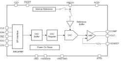
That’s where DAC ICs such as Texas Instruments’ 16-bit DAC81401 and 12-bit DAC61401 (DACx1401) excel (Fig. 1). These devices are pin-compatible, single-channel, buffered, high-voltage output DACs that have a 2.5‑V internal reference with drift of just 10 ppm/°C. They don’t include a lot of extraneous “bells and whistles,” but instead are tightly focused on their primary role.
These devices, based on the well-known R-2R DAC topology, are specified to be monotonic and provide an exceptional nonlinearity of less than ±1 LSB (maximum), coupled with ultra-low glitch energy of under one nanovolt-second (nV-sec). Applications include semiconductor test and ATE, lab and field instrumentation, precision analog-output modules, and servo drive-control modules.
The high-voltage DACs offer user-programmable bipolar output voltages of ±20, ±10, and ±5 V, along with full-scale unipolar output voltages of 40, 10, and 5 V. A power-on-reset (POR) circuit powers up the DAC output and keeps the device in power-down mode until the outputs are enabled to avoid random power-up output voltages.
The DAC double-buffered architecture allows for data updates without disturbing or glitching the existing analog output. Data updates are performed asynchronously. In the update mode, a minimum wait time of 2.4 μs is required between updates of the output.
Communication to the devices is done via a 50-MHz, 4-wire serial SPI-compatible interface supporting 1.7‑ to 5.5‑V operation. If the device is used in a noisy environment, CRC polynomial-based error checking can be invoked by the user to check the integrity of SPI data communication between the device and the host processor.
The DACx1401 devices are fully characterized for operation over the temperature range of –40 to +125°C, offered in a small, 20-pin TSSOP package. The 50-page datasheet provides comprehensive specification and applications insight.
There’s also a schematic and fairly detailed discussion of a higher-voltage analog-output circuit based on these DACs, which adds additional active and passive components to reach 0- to 81-V unipolar/±41-V bipolar operation. For those who are serious about this circuit, an even more-detailed discussion is presented in a nine-page application note.1
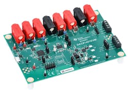
Potential users of even a basic-function IC such as this DAC can benefit from an evaluation unit. The DAC81401EVM is an easy-to-use platform for evaluating the functionality and performance of the DAC81401 (Fig. 2).
This EVM, with its own 29-page user manual, connects to a Windows-compatible PC and is exercised (setup, operation, evaluation) using a graphical user interface (GUI) application that can be downloaded from TI’s website.
Reference
1. “High-Voltage Gain Stage Design Circuit for DAC81401,” Analog Engineer's Circuit SLAAED7, Texas Instruments.


