Silicon-Based Electro-Optical Device Delivers Narrowband Multi-GHz Filtering
This article is part of the TechXchange: Silicon Photonics.
What you’ll learn:
- How an electro-optic PIC can implement RF filtering functions.
- Which E-O components are needed for passband and notch filtering.
- How the overall device was fabricated and the test results.
It’s a very safe bet that a wireless or wired system uses at least one filter—and likely many more—in their various forms: low-pass, high-pass, notch, or bandpass. As operating frequencies increase into the gigahertz and tens of gigahertz range, it’s increasingly difficult to create filters with narrow bandpass or notch performance, especially using discrete-device versions which are almost always impractical in that range.
While there are ways to create such filters using surface-acoustic-wave (SAW) and bulk-acoustic-wave (BAW) technologies, even these technologies struggle to keep up with the demands for narrow bandwidth filtering at these ever-higher frequencies.
Chalcogenide Glass + Silicon
Recognizing the need and opportunity, the photonic and electro-optical (E-O) community is doing a great deal of research to overcome these barriers. For example, researchers at the University of Sydney (Australia) Nano Institute devised a compact semiconductor chip that provides for the heterogeneous integration of chalcogenide glass with silicon to create specialty filters.
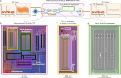
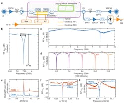
Their effort has resulted in a notch filter with narrow 37-MHz 3-dB bandwidth and deep 51-dB RF rejection, tunable from 2.5 and 15 GHz (Fig. 1). Chalcogenide glass contains one or more chalcogens (sulfur, selenium, tellurium) but excludes oxygen—they have high optical transparency in the infrared (IR) region of telecommunication windows of 3 to 5 μm and 8 to 12 μm.
1. Heterogeneous integration of As2S3 waveguides and silicon components for an on-chip microwave photonic filter system: (a) High-level schematic of the integrated Si-As2S3 MWP notch filter. An RF input signal is modulated onto an optical carrier by a modulator on the Si-As2S3 chip. The modulated optical signal is then processed and undergoes photodetection. The notch filter response is visualized in the RF output spectrum where the spectral component at f1 is attenuated, whereas the signal at f2 is not. (b) A picture of the Si-As2S3 PIC containing (c) a silicon E-O modulator and circuits used for optical carrier control and (d) false-colored optical microscope image of As2S3 spiral waveguides used for Brillouin processing. (PIC: photonic integrated circuit; E-O: electro-optic; CSR: carrier-to-sideband ratio; TC: tunable coupler; TPS: tunable phase shifter; VOA: variable optical attenuator)
Their 5- × 5-mm device integrates As2S3 chalcogenide waveguides in a CMOS foundry-manufactured silicon-photonic chip containing integrated active E-O modulators and photodetectors. The waveguides provide stimulated Brillouin scattering (SBS), which is an optical nonlinearity demonstrated in 1922. The first demonstration of SBS in a photonic chip in 2011 sparked interest in using it for integrated microwave-photonic (MWP) filters with fine spectral resolution.
Filter Process and Test Results
The signal path begins with a two-tone RF signal (frequencies f1 and f2) as input to the MWP filter. After filtering, one tone is attenuated, which is indicated by the spectrally selective notch response. The E-O modulator shifts the RF signal to the optical domain and enables flexible control of the optical carrier-sideband ratio (CSR) and sideband phases. The chalcogenide Brillouin waveguide facilitates fine-spectral resolution processing. Their test setup and results indicate that the design exceeded the anticipated performance (Fig. 2).
2. Si-As2S3 MWP notch filter: (a) Experimental setup. (b) Measured RF notch-filter response with the narrow 3-dB bandwidth of 37 MHz and large 51-dB rejection annotated. (c) Measured RF response of the MWP notch filter with a notch at 8 GHz. (d) Notch filter frequency tuning. The notch frequency is changed between 2.5 and 15 GHz. (e) Measured optical spectra for two different CSRs. Optical processing on the Si-As2S3 PIC reduces the CSR from CSR1 (blue) to CSR2 (orange). The modulated sideband is offset by 7 GHz from the optical carrier. (f) Measured RF response for notch filters with CSR1 and CSR2. (g) Measured notch and bandpass filter responses. A bandpass response can be created by changing the DC bias of the on-chip DDMZM such that the photocurrents destructively interfere outside the Brillouin resonance. (L: laser; EDFA: erbium-doped fiber amplifier; PC: polarization controller; C: circulator; TC: tunable coupler; VOA: variable optical attenuator; TPS: tunable phase shifter; DDMZM: dual-drive Mach-Zehnder modulator; BPF: bandpass filter)
The flexibility of MWP signal processing is made even more apparent when using the on-chip E-O modulator to alternate between bandpass and notch responses. They reconfigured the filter response between notch-mode (blue) and bandpass-mode (orange) filter responses by changing the modulator bias. For a bandpass response, they set the sideband amplitudes to be equal outside the Brillouin resonance, such that the photocurrents destructively interfere.
The work is detailed in their comprehensive yet readable nine-page paper “Integrated microwave photonic notch filter using a heterogeneously integrated Brillouin and active-silicon photonic circuit” published in Nature Communications. Their 19-page “Supplementary Information” provides even more insight.
Read more articles in the TechXchange: Silicon Photonics.
References
“An Introduction to Chalcogenide Glasses,” Springer Link.
“Chalcogenide Glass,” Science Direct.
“Stimulated Brillouin scattering,” University of Central Florida.
“Brillouin Scattering,” Wikipedia.


