This design idea describes a high-current (up to 8 A) shunt-regulator built around the TLV431 low-voltage, adjustable, precision shunt-regulator IC. Special attention was paid to implementing this design as a "two-terminal" circuit block, greatly increasing the versatility of the design. The circuit block can be conceptualized and implemented in any application where a power Zener diode would be used. However, this circuit has much greater precision, accuracy, and range of operational currents than such a diode.
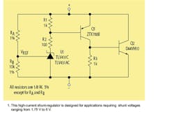
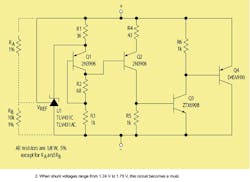
Two circuit varieties are described, based on the voltage range desired. For shunt voltages ranging from 1.75 V to 6 V, the circuit in Figure 1 can be used; for voltages between 1.24 V and 1.75 V, the circuit of Figure 2 must be used.
Both circuits exploit the best features of the TLV431 shunt-regulator—very low operational bias current levels (80 µA max.), and a precision reference voltage (1.24 V). These two features allow the circuits to regulate accurately over a wide range of currents. The circuit shown in Figure 1 will regulate precisely with shunt currents as low as 200 µA and as high as 8 A. That's a 91.8-dB dynamic range. The Figure 2 circuit will regulate with shunt currents as low as 1 mA (at 1.24 V) and as high as 8 A (a 78-dB dynamic range).
The circuits can be used anywhere a power Zener diode function would be utilized. Some typical applications are:
- A high-current (up to 8 A) precision shunt-regulator ("power zener").
- A precise +3.3-V/8-A power supply derived from regulated +5 V.1
- A precision, high-current voltage clamp for overvoltage protection of dc power supplies.
The reason for the two different circuit implementations (Figs. 1 and 2) is the compliance voltage range of the cathode terminal of the TLV431. The cathode terminal can reach as high as 6 V, but can only go approximately 200 mV below the reference voltage (1.24 V) while sinking current. For shunt voltages of 1.75 V up to 6 V, implemented using the circuit of Figure 1, the cathode voltage need only go as low as VSHUNT - VBE. So for VSHUNT = 1.75V, and VBE = 0.6V, VCATHODE will be 1.15 V. This is within the cathode's operational voltage range.
Operation of the circuit in Figure 1 is as follows: For voltages below the shunt voltage, only the bias current of the TLV431 will be drawn. The voltage developed across R1, due to this bias current, won't be sufficient to turn on Q1. Thus, Q1 and Q2 will be off. As soon as the shunt voltage increases to the point where VREF reaches 1.24 V (defined by the resistive divider consisting of RA and RB), the TLV431 will begin to sink current at its cathode terminal. This current will turn on Q1, which in turn drives Q2. As a result, the collector currents of both these transistors are controlled by U1. The total shunt current (ISHUNT) = ICATHODE + IcQ1 + IcQ2. Also, ISHUNT = ICATHODE (ßQ1)(ßQ2). The high Beta (ß = 400 min.) of Q1 makes a Darlington transistor unnecessary. It also allows lower voltage operation, since the extra VBE drop of a Darlington is avoided.
For shunt voltages less than 1.75 V, the circuit of Figure 2 should be used. This circuit allows shunt voltages as low as the reference voltage (1.24 V) to be tightly regulated, with shunt currents ranging from 1 mA up to 8 A. The main difference between the two circuits is that the current-mirror consisting of Q1 and Q2 allows Q3 and Q4 to be fully driven with just a 150-mV range of cathode voltage. Thus, the cathode voltage of the TLV431 drops just 150 mV below the reference voltage when regulating a shunt voltage of 1.24 V.
Operation is as follows: For shunt voltages below the set point, a bias current will flow through Q1, R1, R2, and R3. The bias current flowing through R2 creates an offset voltage that keeps Q2 off. This, in turn, keeps Q3 and Q4 off. When the shunt voltage is high enough so that VREF reaches 1.24 V (defined by resistive divider RA and RB), U1 will start to sink cathode current.
This cathode current will create a voltage drop across R1, causing Q1's emitter voltage to drop. The voltages on the base and collector of Q1 will follow the emitter. When the voltage at the collector of Q1 drops low enough, it will begin to turn on Q2. Then Q3 and Q4 will be driven just as Q1 and Q2 of Figure 1 were driven. (Note: Q3 and Q4 of Figure 2 are complementary devices to Q1 and Q2 of Figure 1). A drop across R1 of 150 mV maximum is sufficient to cause 8 A of shunt current to flow. Q2 of Figure 1 and Q4 of Figure 2 must have a heat sink suitable for their level of power dissipation, given by PD = (ISHUNT)(VSHUNT).
Reference:
- "Single IC in TO-220 Case Converts 5-V Rail to 3.3 V," electronic design, December 17, 1992, p. 37.


