Article updated 9/26/22
Current-feedback (CFB) op amps have earned their reputation in many applications that need bandwidth, without compromising other noise and high-speed characteristics. They have served these needs adequately since the mid '80s, especially where dual supplies and higher voltages are easily available. Concurrently, op-amp suppliers have continued to polish this CFB topology to serve many emerging requirements where very high slew rates, coupled with wide bandwidth, are desired as the gain is increased. Nevertheless, CFB op amps are still far from perfect.
Many emerging portable systems demand higher performance with low power and single-supply operation. At supply currents of 2 mA and below, CFB op amps in particular have one major limitation: bandwidth depends on gain. Like their voltage-feedback (VFB) counterparts, CFB op amps with supply currents under 2 mA feature a bandwidth that varies inversely with gain.
Engineers at Texas Instruments' (TI's) Burr-Brown division have now come up with a novel design that virtually eliminates low-power CFB op-amp bandwidth dependence on gain. Key is modifying the op amp's input buffer stage. TI has used this technique to develop a new family of wideband CFB op amps. Called CFBplus, these op amps unshackle the gain from the bandwidth. Implemented in TI's 15-V complementary bipolar process with integrated CMOS, also called CBC, single-supply operation for the op amps is 5 to 12 V, while the dual supply range is up to ±6 V.
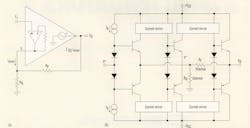
In the new modification, the conventional open-loop buffer, between the noninverting and inverting input nodes, has been transformed into a low-power closed-loop architecture (Fig. 1). A significant reduction of the inverting input impedance results, without sacrificing power.
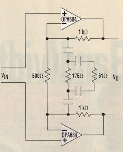
This independence of gain and bandwidth will enable the CFB op amps to support a number of previously difficult applications. For in-stance, adding RC elements in the gain-setting path to provide gain peaking over frequency without interacting with the amplifier's bandwidth is now a reality. This is particularly useful in the differential driver or receiver stages to equalize the high-frequency attenuation for signals in the twisted pair lines.
Providing greater flexibility in gain settings will give amplifiers a greater number of channels. Likewise, an adjustable-gain stage will permit an amplifier to hold the bandwidth constant over gain. Ultimately, the designer decides which way to apply this new component.
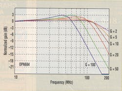
The first two members of the CFBplus family include the OPA683 and OPA684. Internal measurements of the OPA684, which offers 1.8-mA/channel quiescent current, indicate that it achieves over 124-MHz small-signal 3-dB bandwidth from gains between 2 and 20. These results were measured for a load of 100 Ω and a 200-mV p-p output. For gains of 50 and 100, the 3-dB bandwidth drops to 93 MHz and 70 MHz, respectively (Fig. 2).
Bandwidth variation is about 2.5:1 for the 50:1 gain range with a fixed feedback resistor. "Though this still isn't a perfect gain-bandwidth independence, it's far superior to existing low-power CFB op amps," says Michael Steffes, TI's strategic marketing manager for high-speed signal-processing products. "By comparison," he adds, "to obtain similar performance at a gain of 100 from a VFB part, the designer would require a 7-GHz gain-bandwidth product."
Modified Input Stage This gain-bandwidth dependence arises because the input impedance looking into the inverting input of the op amp is nonzero. In the traditional CFB topology, a voltage buffer exists between the two inputs with a low-impedance path on the inverting node for the feedback-error current."As a result, this previously second-order effect becomes a first-order gain-bandwidth dependence for any conventional CFB op amps operating at less than 2 mA of supply current," Steffes explains. "In this topology, the feedback transimpedance that determines the frequency response for a CFB op amp has a term that's the inverting input impedance times the noise gain. For low-power parts, this inverting input impedance becomes quite large. It becomes a dominant term in the loop-gain equation, giving all present low-power CFB parts gain-x-bandwidth dependence characteristics."
The new CFBplus amplifier transcends this limitation by adding internal feedback around the input stage buffer to drive its output impedance lower while retaining the benefits of very low total quiescent power. For example, a typical 2-mA CFB op amp may have 200 µA of bias current in the inverting node, giving a buffer output impedance of about 65 Ω. The new closed-loop input buffer employed in the CFBplus amplifier uses a similar level of quiescent current, but it provides only 5 Ω of impedance looking into the inverting input.
At very high gains, however, this bandwidth independence will be lost due to the loop-gain roll-off characteristics of the closed-loop buffer. The buffer's output impedance starts increasing at very high frequencies. One can overcome this problem by extending the buffer bandwidth at least five times the desired overall closed-loop bandwidth. But this improvement comes at the cost of more power consumption in the buffer stage.
An added benefit of the reduced impedance at the inverting node is the linear error-current sensing operation. Consequently, the new CFBplus op amps push distortion levels much lower than previous CFB amplifiers (see the table). This improvement is noticeable at lower frequencies where the output stage is no longer the dominant contributor to harmonic distortion.
Compared to other CFB op amps, the CFBplus offers over 10 dB of improvement in total harmonic distortion (THD) for a gain of 2 using a 100-Ω load at 2-V p-p output. This performance gap is even higher for higher gains under similar conditions.
In a conventional CFB op amp with a traditional topology, there's a dramatic drop in distortion performance at high gains due to high inverting-node input impedance. Also, as the load increases to 1 kΩ, the CFBplus' distortion performance significantly improves.
Similarly, noise characteristics of the new device are low. Maximum input voltage noise performance is specified at about 3.2 nV/—Hz at frequencies above 1 MHz. The slew rate is better than 800 V/µs. Simultaneously, the output stage of the new op amp has been improved to obtain sufficient headroom to handle large voltage swings at high output currents. Plus, this capability minimizes distortion at higher frequencies. Its dynamic performance has also been enhanced.
CFBplus op amps ensure that the amplifier can deliver adequate bandwidth and output voltage to drive short-loop ADSL lines. Consequently, a dual-channel version with few external passives can be configured as a low-power wideband, differential pre-emphasis line driver (Fig. 3). In conclusion, these improvements make the CFBplus op amps suitable for a variety of applications below 50 MHz.
This article appeared in Electronic Design, Oct 29, 2001.


