The ABCs Of ADCs
What you'll learn:
- What is an analog-to-digital converter (ADC)?
- What are the key performance features of an ADC?
- The different ADC architectures.
Real-world applications require real-world connections. Generally, that means an analog signal is being digitized somewhere in the system so a microprocessor, ASIC, or FPGA can gather data and make some decision. If you’re new to data converter concepts or if it’s been a long time since your last analog class, the datasheet and design specifications and considerations can seem alien or even outright confusing. So what do all of those acronyms mean, and why should you care about spurious-free dynamic range (SFDR) or anti-aliasing?
Primary Selection Criteria
In general, most designers seem to care about several primary criteria when selecting an analog-to-digital converter (ADC). Specs such as power consumption may be very important when designing a next-generation, portable, low-power data-acquisition system. But in most cases, engineers start looking at parts based on:
- Digital interface (SPI, I2C, parallel, etc.)
- Resolution (the amount of effective bits needed)
- Speed of conversion required
- ADC architecture • Input structure (what the analog signal looks like)
Secondary selection criteria usually include power-consumption considerations (active and sleep mode) and reference-voltage integration. They also frequently include system-friendly features, such as an integrated FIFO for the digital data, an integrated programmable gain amplifier (PGA), or general-purpose I/O connected to the serial bus.
Digital Interface Choices
The digital part of an ADC is usually a primary criterion. That’s because the digital system implementation may be limited by the availability of certain interface types as well as required data-transfer rates.
For example, when interfacing an ADC to your favorite microcontroller (with your 10 years of legacy code), you may only have an I2C interface available on the ADC. Or for higher-speed or higher-resolution ADCs, a parallel interface may be the easiest way to rapidly transfer a large amount of data for applications such as digital filtering that might be running inside an FPGA.
Each of the three main interface types—two-wire or I2C, three-wire or SPI, and parallel—offers advantages and disadvantages when they’re offered on precision ADCs. High-speed ADCs (greater than 10 Msamples/s) also may offer low-voltage differential signaling (LVDS) as an interface for high-speed serial connection to an FPGA.
The two-wire or I2C interface offers low pin count and, as a result, small package size. In other words, only two pins are used for data transfers. This allows for maximum channel counts in very small packages. For instance, an eight-pin package provides two pins for the interface, two pins for power, and four pins for analog inputs. The MAX11613 four-channel, 12-bit ADC from Maxim, for example, comes in a micro-max eight-pin package.
The small form factor of these devices makes them ideal for consumer applications and system power-monitoring applications. (I2C also is very similar to power-management SMBus protocols.) In addition, space-constrained applications using three-axis accelerometers and gyroscopes such as game controllers and dead-reckoning systems often use I2C-based ADCs due to their high channel count per unit area.
However, these interfaces provide slow data transfer, and they’re difficult to isolate. The data pin on I2C interfaces is a bidirectional open-collector pin. As such, it may become difficult to use the interface with systems that require (optical) isolation for noise isolation or safety, such as medical applications. In addition, I2C based systems can be slow. Their maximum data-transfer rates usually don’t go above 3.4 Mbits/s.
Three-wire interfaces and SPI deliver a full-duplex, high-speed bus that supports 100 Mbits/s (in theory). Also, if multiple ADCs (or other SPI devices) are on a single bus, you can cascade, say, eight MAX11040 parts for 32 channels on a single isolated SPI bus for power-grid applications. Furthermore, SPI supports easy and cost-effective (optical) isolation. This approach is relatively easy to implement in FPGAs as well. It requires more pins than I2C, though.
Parallel interfaces provide high throughput plus a simple logic control interface, which is good for FPGAs. Unfortunately, they also require a high pin count.
ADC Resolution
So how many bits do you need? This trivial question can be complicated by inherent ADC errors, signal amplitude, least-significant-bit (LSB) step-size, and dynamic range requirements. Simple system voltage and current measurements may require only an 8-, 10-, or 12-bit ADC, for instance. But measuring a sensor in a classic resistive bridge configuration may require a 24-bit sigma-delta ADC device to detect small signal changes in a very large overall signal.
The resolution often is quoted in dB (decibels), which provides an approximation of the overall signal-to-noise ratio (SNR) of the ADC (and hence how small a signal it can resolve from the sensor or system noise floor).
Each bit of resolution is approximately 6 dB. Therefore, theoretically, a 12-bit ADC should have an approximately 72-dB SNR. In reality, many factors limit SNR, and a 12-bit ADC with an SNR of 70 dB or greater would be considered good.
ADC suppliers quote this figure of merit in one of two common forms: effective number of bits (ENOB) or signal to noise and distortion (SINAD). These two forms are related. One definition for ENOB is:
ENOB = (SINAD – 1.76)/6.02
where all values are in dB. SINAD is the ratio of the wanted signal (the fundamental) to the sum of all distortion and noise products, after the dc term is removed. Also:
SINAD = (rms SIGNAL/rms NOISE)
With a perfectly linear (no distortion) but noisy system, SINAD and SNR are interchangeable. Let’s look at a simple example for the MAX1240, a 12-bit, one-channel ADC. The datasheet gives SINAD as 70 dB worst case, so following the formula above, we get an ENOB of:
ENOBMAX1240 = (70 – 1.76)/6.02 = 11.34 bits
Noise sources and harmonics can wreak havoc with the quality of your ADC. Many the system and in the ADC. We’ll look at some of the common sources later on in this article.
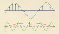
So before deciding how many bits are needed, consider system and ADC errors such as noise and harmonics and ensure that there’s enough resolution even when error is taken into account. If the resolution isn’t high enough, quantization errors occur in the data read, and system accuracy will be compromised (Fig. 1).
Speed of Conversion Require
When determining the required speed of the ADC, several factors must be addressed. However, they all have their roots in Nyquist theory. If you missed that thrilling lecture, here’s the executive summary. To recreate a true representation of a signal, it must be sampled at regular intervals with at least twice the frequency of the highest-frequency signal you’re interested in looking at:
fSAMPLE > 2 * k * fSIGNAL(MAX)
where k > 1 is the over-sampling factor.
The 2× number is called the Nyquist frequency. Figure 2 illustrates a simple example. The green line shows the signal being measured. In the first case, a real representation of the signal is achieved with greater than two samples per cycle. In the second case, undersampling leads to a false representation of the signal. Good design practice in most systems results in the signal being oversampled at least three to four times the highest frequency of interest.
Here’s a simple application example. In a system power-monitoring application, the signal being digitized is usually dc except during power-up, power-down, and fault conditions. Under fault conditions, maybe a response in 1 ms is required. Sampling at, say, 10 ksamples/s per channel allows for an 80-ksample/s, eight-channel ADC to monitor four currents and four voltages with 10 times oversampling to ensure that fault-condition requirements can be met.
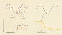
So what happens if the signal input frequency (or a portion of the input frequency) exceeds the Nyquist frequency of the ADC? This isn’t good, and it results in noise in the harmonics frequencies of the signal being looked at. This is called aliasing (Fig. 3). ENOB is a function of signal-to-noise and distortion, so ENOB will suffer if the signal contains components that exceed the Nyquist frequency of the ADC.
To address this issue, a low-pass antialiasing filter is typically used to filter out signals outside of the frequencies of interest before the ADC digitizes the signal. (The input bandwidth of the ADC will also have an effect on harmonic distortion, as will the linearity of the ADC’s transfer function—we’ll have more on these topics in a later article online this fall at www.electronicdesign.com.)
Anti-Aliasing Filters
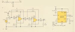
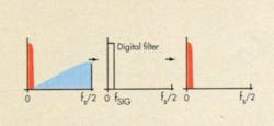
Anti-aliasing filters limit the input to an ADC to the area of signal interest. They attenuate the frequencies that aren’t of interest and may cause harmonic distortion (Fig. 4). Anti-aliasing filters can be constructed using three basic solutions: simple R-C filters, active filters using operational amplifiers and passives, and monolithic switched-capacitor filters.
Simple R-C filters offer a basic design with few components. Their transfer function has one pole. They may not have steep enough attenuation to cut off all unwanted frequencies, though. Additionally, they depend on the accuracy of passives used and are especially sensitive to errors due to component drift over temperature.
Active filters using op amps and passives provide better performance than passive filters. However, they may need several op amps and passives. Also, their performance is still susceptible to the accuracy of the passives used, especially temperature drift. They consume more power as well.
Monolithic switched-capacitor filters require fewer components, less space, and less power than op-amp solutions. Additionally, they offer greater performance and better matching over temperature. They don’t require high-precision external passives. And, these easy-to-use filters come in large families with preset transfer functions.
Switched-cap filters, available as highorder (fifth and eighth order) elliptical, Bessel, and Butterworth filter types, offer up to 83 dB of attenuation. This provides a desired “brick-wall” filter response that’s otherwise very expensive to achieve with op-amp-based solutions.
Speed Verus Power in ADCs
When power matters in a design, many engineers’ first choice for power savings is to slow the clock down. While this may make logical sense, it’s not always the best solution for minimizing system power. If the ADC can be used in a burst mode in the application, this can be the best way to minimize both the ADC power and the power used by the MCU or FPGA that’s connected to the ADC.
Power savings are possible by exploiting the power-down modes of the ADC (and the digital subsystem) and using both the ADC and the MCU in a burst mode. Doing so, the ADC can sleep for most of the time, only powering up for short periods. In many ADCs, the active power, even at slow clock rates, can be 100 times the sleep-mode power.
Running an ADC at higher sample rates for shorter periods may be a good option for periodic data acquisition. Clearly, for mission-critical systems, this technique may not work. In that case, choosing an ADC with the lowest active power consumption makes the most sense.
ADC Architecture
Five basic ADC architectures are used for most commercially available ADCs today: flash (or parallel), successive approximation register (SAR), sigma-delta (or delta-sigma), dual slope, and pipeline.
The flash or parallel ADC includes 2N – 1 high-speed comparators (Fig. 5). These converters typically offer the highest conversion speed and are used where power consumption isn’t a primary concern. Flash ADCs are usually more expensive than most other converter approaches, and their chip area and power consumption generally increase exponentially with resolution.
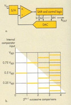
SAR is a binary search approach using a DAC. A comparator forms the basis for these popular ADCs (Fig. 6). After a sample of the analog input is taken, usually by sampling the signal with a capacitor, the signal is successively compared to the output of a DAC to determine each successive register bit. The SAR register sets the DAC input, and the result converges bit-by-bit successively. Conversion time increases with resolution.
Mainstream devices offer medium to high resolution up to 18 bits and an upper range of about 5 Msamples/s at lower resolutions. SAR devices are low-power and have small form factors. Accuracy depends on internal component matching (on-chipbased capacitor arrays). The SAR-based ADC architecture reigns supreme in the marketplace, though sigma-delta devices have become increasingly popular, especially for low-speed, highprecision, sensor-based applications.
SAR devices can be found in a wide array of applications. They include motor control, battery fuel gauges, power-supply and system monitoring, high-speed sensors in automotive power-train and safety applications, rotational sensors, proximity sensors, accelerometers, gyroscopes, protective relays for power systems, and power-amplifier subsystems for communications.
The sigma-delta (or delta-sigma) architecture allows for the implementation of high-resolution to ultra-high-resolution (16 to 24 bits) converters, which are typically low- to medium-speed devices (Fig. 7). In the sigma-delta approach, the converters oversample a signal and then use DSP techniques to shape and filter noise, which achieves excellent SNR in the area of signal interest. It also offers a small die area and typically low speed, usually below 200 ksamples/s.
Simpler analog circuitry is used with a complex internal DSP for filtering and noise shaping. This leads to excellent linearity in the ADC’s response as well as very low harmonic distortion, which are critical for measuring very small signals. The most common application for sigmadelta ADCs other than audio digitization (audio codecs) is the measurement of very small signals from physical sensors. Temperature, weight, pressure, acidity, flow rate, and strain are some of the common physical phenomena digitized by these parts.
The dual-slope architecture provides ultra-low power for measuring slow-moving signals. These dual-slope parts support high resolutions (18 bits). An unknown voltage is integrated, and the value is compared against a known reference that ramps. Sigma-delta devices have replaced this technology in most high-precision applications.
The pipeline architecture supports high speeds to more than 100 Msamples/s and up to 16 bits, with less power than flash. These ADCs are small, pipelined parallel structures in which each stage only works on a couple of bits (Fig. 8). Parallelism increases throughput (speed) at the expense of power and latency (delay). This is a very popular architecture for most high-speed data-acquisition applications, such as RFbased data-acquisition systems.
About the Author

Martin Mason
Director of Precesion ADCs and Filters, Maxim Integrated Products/Analog Devices
Martin has a Bachelor of Engineering from the University of Newcastle upon Tyne in the U.K. He is now Head of Marketing at Blumind AI.


