Hands On: PCBWeb, The Latest PCB Design Tool to Hit the Web
Several browser-based PCB design tools have emerged in the past couple of years, yet the vast majority of designers are still using the same desktop applications that have dominated the EDA industry for decades.
Now PCBWeb, a new design tool from the founders of Aspen Labs, the media company behind the electrical engineering community EEWeb, is the latest product to be introduced into this competitive space. Their goal? To provide a full-featured online circuit design and manufacturing solution for professional engineers.
Aspen Labs is no stranger to developing web-based CAD tools. Last year they launched SchemeIt, a simple electronics diagramming tool, and PartSim, a graphical SPICE simulator. But PCBWeb marks the company’s first introduction of a full-featured design tool, complete with schematic capture and PCB layout.
After two years of development, the product is finally in public beta and available for free. But although the price tag is compelling, PCBWeb shows serious potential to compete with major players based on its technical merit alone, which is in ongoing development.
The company has made an explicit push towards ease-of-use, but make no mistake -- this tool was not designed for weekend hobbyists, says Cody Miller, president and co-founder of Aspen Labs.
“Our goal is not to be an entry-level tool or toy,” says Miller. “Our goal over the next five years is to be a full-featured, serious design tool competitive to mid-level PCB design tools.”
Schematic Capture
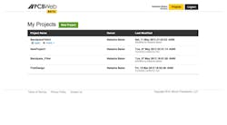
Upon signing into PCBWeb, users can open an existing project, create a new one, or add collaborators to a project (Fig. 1). Each project has three views -- the schematic, PCB layout, and bill of materials (BOM). For the purpose of testing the product, I decided to capture and lay out a simple bandpass filter.
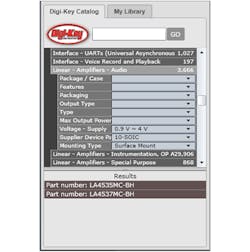
The parts library contains over 100,000 parts arranged by category. There is parametric search built directly into the parts database (Fig. 2), and hovering over a part displays its characteristics, such as the manufacturer, mounting and package type, RoHS compliance, and the part’s electrical specifications, such as gain bandwidth product and operating temperature.
Related Articles
• The Rise Of The Online Circuit-Design Collective
• What’s New in Eagle V6 PCB Design Software? Prepare for More Third-Party Tools
• PCB Technology Interview With Sunstone
When starting to place parts, the first thing that struck me was that the app operates very much like a native desktop application. There is no noticeable lag time, and standard commands are supported (such as Ctrl+C and Ctl+V to copy and paste or left-clicking for additional options).
Currently all parts in the database are real orderable products; there are no generic parts for things like passives, which are sometimes nice to specify later after tweaking values. This is coming very soon according to Aspen Labs’ CTO Joe Wolin, as is the ability to control when parameter values of passives are displayed on the schematic.
If a symbol is not available in the database, users can create one.
The schematic environment, which supports multi-sheet design and multi-section components, is modeless—meaning it tries to predict what the user wants to do—whether that’s move a part or place a wire, based on where they hover, rather than requiring users to select filters. This is an ease-of-use feature that Miller said is important in a tool that is used daily. Wiring of parts is also nice; moving around a part does so without breaking wires or creating strange rewiring.
PCB Design
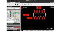
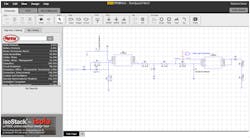
After completing the schematic (Fig. 3), clicking on the PCB tab will instantly display the parts and rats nest on the layout. The PCB layout supports multi-layer boards (up to 30 layers), as well as DRC. There is not yet an autoplacer, but this is high priority on the company’s roadmap, as is an autorouter.
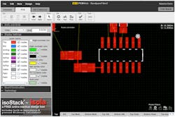
Users can move parts to different layers, and toggle between layers for part placement and routing. There are also filters to help select objects such as parts, pads, traces and polygons on layers, which are helpful for dense designs (Fig. 4). Making changes to the schematic updates the layout as would be expected.
The PCB layout also supports copper pours and planes, and several other features such as high contrast mode to help see traces on a particular layer. The company also plans to implement impedance control calculators and other tools.
Currently, creating a footprint is a bit difficult and needs to be done pad by pad, but the company plans to launch a new component wizard this month.
Finalizing a Design
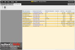
Upon completion of a design, parts can be ordered through direct integration with Digi-Key using the order button in the BOM (Fig. 5).
Gerber files can also be generated by clicking on “Order Boards.” In the future, the company intends to partner with manufacturing houses to make it easier for engineers to manufacture boards, as well as serve as a revenue stream for the company.
Other Notable Points
Being able to fire up a browser and have all of your projects readily available in the cloud is liberating. However, occasionally browsers crash or a page is accidently refreshed; luckily the tool was able to recover unsaved changes in several instances when this happened.
Sharing a design is another nice feature of the tool. A design can be shared by making it global and sharing a link, or by inviting specific collaborators. Of course, the default setting is to keep things private.
“We feel that being able to share things online is going to be very effective and people will embrace that,” said Miller, noting that it could be used to hand off a project between the design and layout stages.
It could also be an interesting way to share hardware designs. A design could be ordered based on its Gerber files ‘as is’, or customizations could be made.
The company also plans to release a scripting feature, similar to Eagle’s user language programs (ULPs), which could be used to execute tasks such as part placement.
One last thing I tried was to open PCBWeb on my iPad—more out of curiosity than anything. Unfortunately Silverlight, the web technology used by the product, only works on Windows and Mac (sorry Linux users but you are out of luck).
Conclusion
PCBWeb shows tremendous potential as a web-based design tool for professional designers. It will have to butt heads though with the likes of Eagle and Diptrace in the desktop software space, and other browser-based tools, namely Upverter, CircuitLab and Circuits.io. Of course convincing engineers that they don’t need desktop software for circuit design will be another challenge altogether for the company.
But Miller is upbeat about PCWeb’s prospects. “Some engineers are excited about [being online] and some have reservations because there’s a different paradigm about using online tools and being able to create your designs in the cloud,” he said. “But as people use it more and more, they’ll become more comfortable with a web app.”
Natasha Baker, founder of SnapEDA, a CAD community for circuit designers, previously worked at National Instruments and consulted for Analog Devices. Baker received a bachelor’s degree in electrical engineering from the University of Toronto, Canada. She can be reached at [email protected].
