Hardening And Testing Semiconductor Devices In The Space Radiation Environment
Space is a challenging environment, particularly due to the intense radiation encountered in nearly all mission profiles. To understand the effects of radiation on electronic systems and components, it is useful to first consider the source of the radiation.
Radiation in space consists predominantly of electrons, protons, and energetic heavy ions. These moderate-energy particles are mostly a part of the solar wind and are anisotropic. Superimposed on this particle flux are very high-energy galactic and extragalactic heavy ions, which are isotropic.
The Earth’s magnetic field traps moderate-energy particles (electrons and protons) in the van Allen belts. Depending on the satellite’s orbit, the belts will cause most of the ionizing radiation damage. The magnetosphere affects high-energy protons and heavy ions as well, but they are much more difficult to trap.
Table Of Contents
• Testing
• Hardening Semiconductor Devices
So how do these particles interact with the materials used in electronic devices? Solar electrons and protons are very abundant and cause ionization in materials. In a simplified model, these charged particles generate hole-electron pairs in the thermal oxides used in ICs.
Related Articles
- Understanding In-Flight And In-Space Radiation Effects On CMOS Devices
- The Straight Poop On Sheltering Astronauts From Cosmic Rays
- Radiation-Hardening Power Devices
The electron mobility in these oxides is very high, and the applied electric field sweeps the electrons out of the oxide in picoseconds. The hole mobility is much less, so a much greater proportion of holes gets trapped. The net result of these asymmetrical trapping dynamics is positive volume charging, with serious effects on the characteristics of both bipolar and MOS devices.
Electron and proton testing is inconvenient and very expensive, though, so the space community has historically used gamma rays for ground testing. It’s a simulation, but we have 50 years of correlation and high confidence using high-energy photons to predict part response to charged particles. 60Co is an inexpensive gamma ray source and is widely used for “total dose” testing, in which the dose rate was eventually found to play a major role.
This file type includes high resolution graphics and schematics when applicable.
Testing had historically been performed at high dose rates in the 50- to 300-rad(Si)/s range, which is a convenient approach as the test takes less than an hour for a 100-krad(Si) exposure. In 1992, research results showed bipolar analog parts to be much more sensitive at dose rates of as low as 0.01 rad(Si)/s. The problem is that the dose rate in space is even lower than that, and the high-dose-rate test hasn’t turned out to be conservative in many technologies.
A low-dose-rate test to 100 krad(Si) takes 20 weeks, which stretches out schedules and increases screening costs. Low-dose-rate hardness has turned into an important hardness assurance (HA) issue, with many users insisting on low-dose-rate testing on a characterization or acceptance basis and deemphasizing high-dose-rate testing.
Intersil Corp. has introduced a low-dose-rate HA program that performs routine wafer-by-wafer acceptance testing at both low and high dose rate using on-site production irradiators. Note that the unit for total ionizing dose is the radiation absorbed dose (rad), which equals 100 ergs per gram. The energy absorption is specific to the material being irradiated, so the common unit in silicon technology becomes the rad(Si).
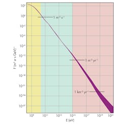
The foregoing discussion considers charged particles of moderate energy, which are abundant in the space environment. As the particle energy increases, the particle abundance will decrease, with the abundance versus energy curve spanning some 25 orders of magnitude and ending up at very low fluxes of relativistic tera-electronvolt (TeV) heavy ions (Fig. 1).
The effects of abundant lower-energy particles are uniform through the volume of the semiconductor chip, while the much less abundant high-energy heavy ions (known somewhat incorrectly as cosmic rays) cause single-event effects, defined as the interaction of a single energetic ion with a silicon device.
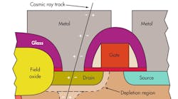
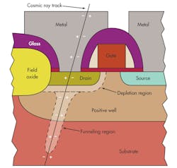
These high-energy particles lose energy as they pass through the semiconductor lattice, generating a dense track of hole-electron pairs (Fig. 2). The resulting charge will be collected by reverse-biased junctions and will be converted into a voltage pulse. This collected charge can change the voltage on sensitive nodes, which can affect circuit operation.
Single-event effects (SEEs) can be divided into destructive and nondestructive phenomena. Nondestructive effects include bit flips, functional interrupts in digital applications, and transients on the outputs of analog functions. The bit flips can be corrected by a rewrite or a reboot, but single-event transients are particularly difficult to deal with in power management applications.
Destructive effects include latchup, burnout, and MOS gate oxide rupture, all of which can lead to permanent damage, nonfunctional parts, and possible mission failure. The most commonly used unit in SEE work is the linear energy transfer (LET) of the incoming ion, which equals the energy loss (dE/dx) per unit track length for a given material density and is expressed in MeVcm2/mg. Heavy ion effects are commonly simulated by using a cyclotron as an ion beam source.
Shielding, then, is ineffective as the particle energy can be in the giga-electronvolt (GeV) range. It filters out the low-energy end of the spectrum only. The high-energy ion flux is unaffected, and mitigation must hence be performed at the component and system levels.
Hardening Semiconductor Devices
Hardening space systems to total ionizing dose and SEEs requires attention at all of their levels. Total ionizing dose causes parametric degradation in semiconductor parts, and this is particularly difficult for bipolar analog parts in the low-dose-rate environment.
Single-event transients (SETs) in continuous-time analog signal chains can cause inaccuracy and system disruption. These transients can be filtered out using low-pass filter functions, but the transient duration must be low for this approach to be effective.
As an example of a hardened operational amplifier with superior SET and total dose performance, the ISL70444SEH quad op amp is optimized for maximum dynamic range, rail-to-rail input and output signal range, and predictable SET response. It is designed to operate over a single supply range of 3 V to 36 V or a split supply voltage range of ±1.5 V to ±18 V. It has demonstrated excellent performance in the total dose and SEE environments, including low- and high-dose-rate total dose testing and destructive and nondestructive SEE testing.1
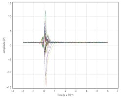
Typically, SET waveforms are obtained at an LET of 86.4 MeV.cm2/mg. Superimposing a number of these waveforms plotted on one common set of axes forms an “envelope” that allows evaluation at a glance (Fig. 3). The ISL70444SEH is built using the Intersil PR40 dielectrically isolated (DI) complementary bipolar process, which has shown excellent total dose and SEE hardness.2
The passively isolated structure eliminates single-event latchup and supports vertical PNP transistors instead of the more commonly used lateral devices. The total dose sensitivity of lateral devices is well known. The PR40 process is Qualified Manufacturers List (QML) certified and in volume commercial production. The ISL70444SEH is available in a 14-lead hermetic ceramic flatpack and is specified from –55°C to 125°C.
As a second example, consider a power-management component that offers improved performance in both the total ionizing dose and SEE environments. The ISL75052SEH is a radiation-hardened, single-output low-dropout regulator (LDO) intended for low-voltage, high-current applications such as FPGA power management. It is specified for an output current of 1.5 A over an input voltage range of 4.0 V to 13.2 V and an output voltage range of 0.6 V to 12.7 V.
The use of a P-channel MOSFET pass transistor enables dropout voltages as low as 75 mV typical (at 0.5 A). When enabled, the ISL75052SEH operates with a low ground current of 11 mA (typical), which provides operation with low quiescent power consumption. The device is stable with tantalum capacitors as low as 47 μF (KEMET T525 series) and provides excellent voltage regulation from no load to full load.
The ISL75052SEH is designed for predictable operation in the SEE environment, including reduced output single-event transient (SET) magnitude. Extensive SEE testing has been performed at Texas A&M University.3 The part has also shown excellent stability over 60Co irradiation to 150 krad(Si) at low and high dose rates.4 It is built in the Intersil P6 process, a submicron BiCMOS process optimized for power management applications.
Available in a 16-lead hermetic ceramic flatpack and in die form, the ISL75052SEH offers guaranteed performance over the full –55°C to 125°C military temperature range.
1. van Vonno, N.W., Williams, B., Hood, R., Thomson, E.J., and Bernard, S.K., “Total Dose and Single Event Effects Testing of the Intersil ISL70444SEH Hardened Operational Amplifier,” 2013 IEEE Radiation Effects Data Workshop Record, July 2013
2. van Vonno, N.W., Pearce, L.G., Hood, R., Thomson, E J., Mansilla, O. and Chesley, P.J., “Total dose and single event testing of the Intersil ISL70227RH low-noise operational amplifier,” presented at the 2011 Radiations et ses Effets sur Composants et Systėmes (RADECS) Conference Workshop, Sevilla, ES, September 2011
3. Pearce, L.G., “Single Event Performance of the ISL75052SEH,” http://www.intersil.com/content/dam/Intersil/documents/an18/an1851.pdf, June 2013
4. van Vonno, N.W., “Total dose and anneal testing of the ISL75052SEH low dropout regulator,” http://www.intersil.com/content/dam/Intersil/documents/an18/an1852.pdf, June 2013
Nick van Vonno is a principal engineer in Intersil’s High Reliability products group. He has 42 years of service with Intersil and its predecessors in a number of technical and management posts. He is currently responsible for radiation effects research, customer support, and technology development for the product line. He has a BSEE from the University of Florida and is a Senior Member of IEEE. He received the IEEE Radiation Effects Award in 2009 as well.


