Modern interface isolators integrate interface transceivers with an internal isolation barrier. Older designs, prior to this integration, use separate, standalone isolators in combination with standard interface transceivers to accomplish the same interface isolation. Surprisingly, these legacy designs still offer a significant cost advantage over their integrated counterparts.
Related Articles
- Advanced Digital Isolation Technologies Boost Solar Power Inverter Reliability
- With Proper Isolation, You Won't Need To Do The Safety Dance Around High Voltages
- Capacitive Isolated Gate Drivers Spin AC Induction Motors
The discrete I2C isolator is among the most often considered isolators. This most stubborn, hard-to-die design continues to fascinate many engineers due to its simplicity. Circuit performance, however, changes with variations in temperature and supply, making re-designs inevitable. Still, this effort can be avoided when using an integrated version.
I2C Bus Operation
The I2C or inter-integrated circuit bus is a multi-master bus with two bidirectional signal lines: one for clock (SCL), the other for data (SDA). Bus access is via open-drain outputs (Fig. 1). Both signal lines connect to the bus supply via pull-up resistors. When a node accesses the bus, its open-drain output pulls the signal line to ground potential. This is considered a logic zero. When the same output is high-impedance, the signal line is pulled up to the potential of the bus supply. This is considered a logic one.
Four different speed modes exist: standard mode (100 kbits/s), fast mode (400 kbits/s), fast mode plus (1 Mbit/s), and high-speed mode (3.4 Mbits/s).
I2C specifies two roles for bus nodes. A master node always provides the clock signal and the slave addresses. It also initiates and ends data transfers. A slave node always receives the clock and the addresses from the master and responds to master requests (Fig. 2). If a slave is not ready to respond, it pulls down the SCL line to force the master to wait until the line is released (high) again.
Signal transitions from one logic state to another during a transfer occur when SCL is low. Transitions at the start or end of a transfer occur while SCL is high. While I2C can be used over a wide voltage range, the most commonly used supply levels are 3.3 V and 5 V.
Isolated I2C Bus
I2C buses using separate power supplies for master and slave nodes commonly apply signal isolators between the master node and the slave nodes to prevent the creation of unintentional ground loops (Fig. 3). Using a single ground connection could prove fatal, as this shortens different ground potentials. The resulting ground loop currents can deteriorate the signal integrity of the clock and data signals and even damage bus node circuits.
Integrated I2C isolator
To isolate a bidirectional signal path with unidirectional isolators, an integrated I2C isolator internally splits a bidirectional line into two unidirectional signal lines, each of which is isolated via a single isolation barrier (Fig. 4). Each channel has an open-drain output. Side one of the isolator connects to a low-capacitance I2C master node, typically the bus controller. Side two is designed for connecting to a fully loaded I2C bus with up to 400 pF of bus capacitance.
To prevent the internal signal loop from latching up, the loop is broken at the output of buffer B, whose output low-level (VOL*) of 0.8 V is higher than the 0.4-V output low-level (VOL) of the master node at SDA1. Comparator C has upper and lower input voltage thresholds that distinguish between the 0.4-V low-potential driven by SDA1 and the raised 0.8-V output low-level from B.
Thus, comparator C allows low-level voltages from SDA1 to pass through to SDA2. In the opposite direction, however, it blocks low-level signals created at SDA2 from returning to SDA2, which prevents device latch-up.
Discrete Or Cheapskate Solution
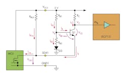
In a discrete I2C isolator, a single transistor performs the comparator function (Fig. 5). While the base terminal assumes the function of the comparator’s reference input, the emitter is the comparator’s signal input SDA1 and the collector is the comparator output.
Take an I2C isolator operating from a 5-V supply and supporting data rates of up to 200 kbits/s. In transmit direction from SDA1 to SDA2, the MCU starts a communication by pulling SDA1 low. Two currents, IPUa through pull-up resistor RPU1 and emitter current IE from transistor Q1, flow together into the open drain of the MCU’s SDA output, creating the low-level output voltage, VOL1.
The current through the pull-up resistor is calculated with:
IPUa = VCC1 – VOL1/RPU1
Limiting the current in the SDA1 line to 1 mA ensures low VOL levels of approximately 100 mV in the output stages of the MCU’s I/O and the isolator IC. Assuming a VOL1 of 0.1 V, a supply of VCC1 = 5 V, and a pull-up resistor of RPU1 = 10 kΩ, IPUa = 490 μA. Letting an equal current flow through Q1 requires a collector resistor of:
RC = VCC1 – VCE–sat – VOL1/IC
With IC ~ IE ~ IPUa, and a saturation voltage of VCE-sat = 0.1 V, the collector resistor RC = 10 kΩ.
A switching transistor chooses a transistor with a minimum forward current gain of ≥ 100. To ensure transistor saturation, the base current should be IB = 50 μA for a collector current of IC = 500 μA. The bias current, IB2, should be approximately 10 times the base current, making IB2 = 500 μA and IB1 = IB2 + IB = 550 μA.
To turn T1 fully on, its base potential must be larger than the maximum base-emitter voltage, plus the low-level output voltage at SDA1:
VB = VBE–MAX + VOL
For T1, VBE-max is given with 850 mV, yielding a base potential of:
VB = 0.85 V + 0.1 V = 0.95 V
At low currents, the forward voltage of a Schottky diode is assumed with VF = 0.3 V. The value of bias resistor RB2 is given with:
RB2 = (VB – VF)/IB2 = (0.95 V – 0.3 V)/500 µA = 1.3 kΩ
Then the upper bias resistor, RB1, can be calculated via:
RB1 = (VCC1 – VB)/IB1 = (5 V – 0.95 V)/550 µA = 7.36 kΩ
Choose the closest resistor from the E-96 series with RB1 = 7.32 kΩ.
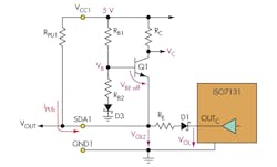
In the receive direction, from SDA2 to SDA1, communication starts when the I2C bus is pulled low at SDA2 and the isolator output, OUTC, turns low.
First, the isolator’s push-pull output must be converted into an open-drain output via diode D1. The output low-level of the isolator is assumed with VOL = 0.1 V, the forward voltage of D1 with VF = 0.3 V. To turn Q1 fully off, a base-emitter voltage of VBE-OFF = 0.4 V is chosen. This requires an SDA1 potential or VOL2 of:
VOL2 ≥ VB – VBE–OFF = 0.95 V – 0.4 V = 0.55 V
To provide a sufficient guard band to VOL1, VOL2 is raised to 0.7 V. The emitter resistor, RE, is calculated via:
RE = (VOL2 – VF – VOL)/IPUb
The current through the pull-up resistor is determined by:
IPUb = (VCC1 – VOL2)/RPU1
Inserting numerical values yields a charge current of:
IPUB = (5 V – 0.7 V)/10 kΩ = 430 µA
and an emitter resistor:
RE = (0.7 V – 0.3 V – 0.1 V)/430 µA = 698 Ω
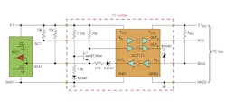
Figure 7 shows the final circuit. Note that the value for the pull-up resistor on side 2, RPU2, is not given as it depends on the actual bus capacitance and the required time constant RPU2 • CB2.
References
Download ISO1540 and ISO1541 data sheets at www.ti.com/iso154-ca and www.ti.com/iso1541-ca.
Thomas Kugelstadt is an applications manager with Texas Instruments. He is responsible for defining new, high-performance analog products and developing complete system solutions for industrial interfaces with robust transient protection. He is a graduate engineer from the Frankfurt University of Applied Science. He can be reached at [email protected].


