As high-speed analog-to-digital converter (ADC) technology improves, so does the need to resolve very high intermediate frequencies (IFs) accurately at high speeds. This poses two challenges: the converter design itself and the front-end design that couples the signal content to the converter. Even if the converter’s performance itself is excellent, the front end must be able to preserve the signal quality too.
Related Articles
- High-Speed ADC Input Impedance: A Measured Versus A Mathematical Approach
- Dissecting The High-Speed Amplifier/AAF/ADC Interface
- Maximize ADC Performance Through Balance And Symmetry
High-frequency, high-speed converter designs exist in many applications today, with radar, wireless infrastructure, and instrumentation pushing these boundaries. These applications demand the use of high-speed gigasample-per-second (GSPS) converters with resolutions of 8 to 14 bits. But remember, many parameters must be met to satisfy the “match” for your particular application.
Laying The Foundation
It is natural to gravitate to GSPS converters for applications such as radar, instrumentation, and communication observation because they offer a wider frequency spectrum or Nyquist band. Wideband, as defined here, is the use of signal bandwidths greater than 100 MHz and ranging into the +1- to 4-GHz frequencies. However, a wider frequency spectrum poses even more challenges on the front-end design.
You can purchase a converter with a +1-GHz Nyquist, but you still have to wrap the right components around it and pay closer attention to the circuit’s construction, i.e., its front end. Challenges escalate when the application calls for +1-GHz super-Nyquist sampling, where spectral information must be captured in the second, third, or fourth Nyquist zone.
Quick Note On Bandwidth
Keep in mind that a converter’s full-power bandwidth is different from converter “useable or sample” bandwidth. Full-power bandwidth is the bandwidth that the converter needs to acquire signals accurately and for the internal front end to settle properly. Selecting an IF and using the converter out in this region is not a good idea since performance results will widely vary in the system.
Based on the rated resolution and performance stated in the converter’s datasheet, the full-power bandwidth is much bigger than the sample bandwidth of the converter itself and possibly twice as big. The design is centered around the sample bandwidth. All designs should avoid using some or all of the highest-frequency portions of the rated full-power bandwidth or risk a de-rating in dynamic performance (SNR/SFDR).
To determine the sample bandwidth of the high-speed ADC, consult the datasheet or application support, since sometimes it isn’t specially given. Typically, the datasheet has specified or even listed production-tested frequencies that guarantee delivered performance within the converter’s sample bandwidth. However, better explanations about these bandwidth terms in the industry need to be specified and defined.
Balun Characteristics & Imbalance
Once the application bandwidth and high-speed ADC are known, choose the front-end topology: amplifier (active) or transformer (passive). The tradeoffs between the two are long and depend on the application.3 This article will concentrate on transformer/balun coupled front-end designs.
The term “balun” will be used in the context that is referring to a transformer or balun. Even though there are differences between the two in their construction and topology, the assumption is that a passive device is used to couple and build the front end, which converts the incoming IF of interest from a single-ended signal to a differential one.1
Baluns have different characteristics than amplifiers and should be considered when choosing the device. Voltage gain, impedance ratio, bandwidth and insertion loss, magnitude and phase imbalance, and return loss are some of these different characteristics. Other requirements may include power rating, type of configuration (such as balun or transformer), and center tap options.
Designing with baluns is not always straightforward. For example, balun characteristics change over frequency, complicating expectations. Some baluns are sensitive to grounding, layout, and center tap coupling. It is wise not to fully expect the datasheet of the balun to be the sole basis for choosing it. Experience can play a huge role here as the balun takes on a new form when printed-circuit board (PCB) parasitics, external matching networks, and the converter’s internal sample and hold circuit (i.e., load)5 also become part of the equation.
Signal gain is ideally equal to the transformer’s turns ratio. Although voltage gains within a balun are inherently noise-free, using a balun with voltage gain does gain the signal noise. There also can be a significant tradeoff in bandwidth as well. Baluns should be viewed simplistically as a wideband passband filter with nominal gain. Therefore, the typical trend is the more signal gain in the balun, the less bandwidth.
Voltage gains with baluns can be highly variable, allowing for more significant ripple and roll-off to be obtained when it isn’t wanted. Finding a 1:4 impedance ratio transformer with good gigahertz performance is difficult today. In summary, be wary. Plans to use 1:4, 1:8, and 1:16 impedance ratio baluns to improve or optimize the noise figure within the final signal chain stage should be well thought out and verified in the lab. Since bandwidth options become limited, as well as performance, the tradeoffs are significant, forcing the performance to be no better than a 1:1 or 1:2 impedance ratio design when designing in gigahertz regions.
The balun’s insertion loss is simply the loss over the specified frequency range and is the most common measurement specification found in any balun datasheet. This will definitely change when implemented in the circuit. Typically you can expect half the frequency range specified in the datasheet. (Yes, that’s right, half.) Some are worse than that, depending on the balun’s topology and sensitivity to load parasitics, such as capacitance. This is probably the most misunderstood parameter about baluns since they are optimized without load parasitics in an ideal impedance situation. In other words, they are characterized with a network analyzer.
Return loss is the balun’s mismatch of the effective impedance of the secondary’s termination as seen by the primary. For example, if the square of the ratio of secondary to primary turns is 4:1, one would expect a 50-Ω impedance to be reflected onto the primary when the secondary is terminated with 200 Ω. However, this relationship is not exact.4
To determine the reflected impedance on the primary changes with frequency, find the return loss at the center frequency specified for the design. This example uses 110 MHz. Zo is found not to be 50 Ω as assumed for an ideal transformer. It is lower, as found in Equation 3:
Return loss (RL) = –18.9 dB at 110 MHz = 20*log[(50 – Zo)/(50 + Zo)] (1)
10^(–18.9/20) = (50 – Zo)/(50 + Zo) (2)
Zo = 39.8 Ω (3)
Next, ratio the primary Zo found in Equation 3 and secondary ideal impedance. Do the same for the primary ideal and solve for the real secondary impedance:
Z(prim reflected)/Z(sec Ideal) = Z(prim Ideal)/Z(sec reflected) (4)
39.8/200 = 50/X (5)
Solving for X:
X = 251 Ω (6)
This example proves a 251-Ω differential termination should be present on the secondary to reflect a 50-Ω load on the primary. Otherwise, the preceding stage in the signal chain ends up driving a heavier load (~40 Ω). This leads to more gain in the preceding stage. More gain and misrepresented load conditions then lead to more distortion that the high-speed converter will “see,” limiting the system’s dynamic range. In general, as the impedance ratio goes up, so does the variability of the return loss. Keep this in mind when designing a “matched” front end with a balun.
Magnitude and phase imbalance are the most critical performance characteristics when considering a balun. These parameters provide a good measure of how each single-ended signal is off from the ideal: equal in magnitude and 180° out of phase. These two specifications give the designer a perspective on how much signal linearity is being delivered to the converter when a design calls for high (+1000 MHz) IF frequencies. In general, the more they deviate, the worse the degradation in performance can be expected.
Stick to those transformers or baluns that publish this information in the datasheet as a start. If the information is not present in the datasheet, it may not be a good choice for this high-frequency application. As frequency increases, the nonlinearities of the balun also increases, usually dominated by phase imbalance, which translates to worse even-order distortions (mainly second harmonic or H2) as seen by the high-speed converter. Even three degrees of phase imbalance can significantly degrade performance in spurious-free dynamic range (SFDR). Don’t be quick to blame the converter. Look at the front-end design first if the expected datasheet spurious is way off, especially H2.
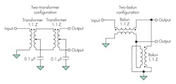
There are some solutions, though, to combat against second harmonic distortions. When using a balun at higher frequencies, try using multiple transformers or baluns in a cascaded fashion. Two or sometimes three baluns can be used to help convert the single-ended signal to differential adequately across high frequencies (Fig. 1). The downside is space, cost, and insertion loss.2
1. Double balun/transformer topologies can mitigate second harmonic problems related to phase imbalance issues.
The other suggestion is to try different baluns. Better single-solution baluns are out there from Anaren, Hyperlabs, Marki Microwave, Minicircuits, and Picosecond, to name a few. Their patented designs use special topologies allowing for extended bandwidth in the gigahertz region, providing a high level of balance that only employs a single device. In some cases, they’re smaller than the standard ferrite footprints commonly used today.
Not all baluns are specified the same way by all manufacturers, and baluns with apparently similar specifications may perform differently in the same situation. The best way to select a balun for the design is to collect and understand the specs of all baluns being considered and request any key data items not stated on the manufacturer’s datasheets. Alternatively, or in addition, it may be useful to measure their performance using a network analyzer or on the system board in front of the high-speed ADC.
Finally, when using a single-balun or multiple-balun topology, layout plays an equally important role in phase imbalance as well. Keeping performance optimized at higher frequencies means keeping the layout as symmetric as possible. Otherwise, slight mis-matches in traces on the front-end designs that use a balun can be proven useless, including dynamic range limiting
Front-End Match
First off, the word “match” is a term that should be used wisely. It is almost impossible to “match” a front end at every frequency today with 100-Msample/s converters, let alone over a band that’s greater than 1000 MHz. The term match should be positioned to mean optimization yielding the best results given the front-end design. This would be an all-inclusive term where impedance, ac performance, signal drive strength and bandwidth, and pass-band flatness yield the best results for that particular application.
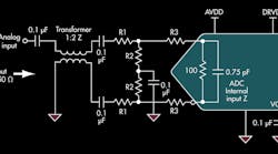
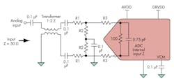
Each parameter, then, should have a particular weight of importance per the application. In some cases, for example, bandwidth (BW) might be the most important spec so other parameters are allowed to suffer a bit if the right amount of BW can be achieved. Figure 2 illustrates the input network for a GSPS converter. Each resistor in the network is like a variable. But as each of these resistor values is varied to create essentially the same input impedance, the performance parameters will change (see the table).
2. Front-end networks can be optimized for bandwidth.
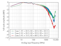
The impedance matching network is roughly the same, but the yielded results between these three examples are different across the measured parameters needed to design the front-end network. The match here is the best result for all the parameters involved where in this case more than 2.5 GHz of BW was required. This narrows the choices down to Case 1 and 2 (Fig. 3).
3. This plot of bandwidth matching shows the differences obtained with different front-end network values.
Case 2 would be more desirable for two reasons. First, the passband flatness only has 2 dB of ripple across the 2-GHz region. Second, the input drive is 3 dBm less than Case 1. This constrains the RF gain less further up the signal chain to achieve full scale of the high-speed converter on the primary of the balun. Case 2 seems to be the best “match” in this example.
Summary
GSPS converters offer ease of use in theory when it comes to sampling wider bandwidth to cover multiple bands of interest or relieve a mix down-stage on the front-end RF strip. However, achieving bandwidth in the +1-GHz range can pose challenges to designing high-performance converter front-end networks.
Keep in mind the importance of specifying a balun where phase imbalance will become important in what the high-speed ADC understands as optimal second-order linearity, for example. Even when a balun is chosen, don’t throw away its performance by using poor layout techniques, and be wary about matching the network properly. Many parameters need to be met to satisfy the “match” for your particular application.
References
1. Transformer-Coupled Front-End for Wideband A/D Converters – Analog Dialogue, April 2005
2. Wideband A/D Converter Front-End Design Considerations – When to Use a Double Transformer Configuration– Analog Dialogue, July 2006
3. Wideband A/D Converter Front-End Design Considerations II - Amplifier- or Transformer Drive for the ADC? – Analog Dialogue, February 2007
4. AN-827, A Resonant Approach to Interfacing Amplifiers to Switch-Capacitor ADCs
5. AN-742, Frequency Domain Response of Switched-Capacitor ADCs
6. AN-912, Driving a Center-Tapped Transformer with a Balanced Current-Output DAC
Rob Reeder is a senior system application engineer with Analog Devices Inc. in the Industrial and Instrumentation Segment focusing on military and aerospace applications in Greensboro, N.C. He has published numerous papers on converter interfaces, converter testing, and analog signal chain design for a variety of applications. Formerly, he was an application engineer for the high-speed converter product line for eight years. His prior experience also includes test development and analog design engineering for the Multi-Chip Products group at ADI designing analog signal chain modules for space, military, and high-reliability applications for five years. He received his MSEE and BSEE from Northern Illinois University in DeKalb, Ill., in 1998 and 1996 respectively.


