Offset Compensation Technique Improves Bridge-Configured Sensor Performance
This article is part of the Ideas for Design Series: Vol. 3, No. 7.
Strain gages and pressure sensors usually are connected in a bridge configuration. These sensors have a typical full-scale sensitivity of 3.0 to 5.0 millivolts per volt (mV/V) of excitation, though some may be as low as 1.0 mV/V. This level is intended to improve linearity while minimizing mechanical stress in the sensor, but at the expense of the signal level.
One way to increase the signal level is to increase the excitation level. But if the system works from a single 3.3- or 5.0-V supply, this may not be an option. Usually, substantial gain must be added to get the signal into the range of a reasonable analog-to-digital converter (ADC).
Related Articles
- What's All This Bridge Amplifier Stuff, Anyhow?
- Use Strain Gauge-Based Sensors Like A Pro
- Solid-State Multiplexers Reduce Half-Bridge Error
Most systems digitize sensor data, then display it or perform some control function. That means a microcontroller is available to control gains and connections. The op amps inside typical microcontrollers have input offset voltages that are higher than what can be used directly in some applications.
For example, with a 5.0-mV/V sensor and 5.0-V sensor drive, full scale is 25.0 mV. An instrumentation amplifier built using op amps with input offset of 3.0 mV uses up to 24% of the available range. Further, an offset drift of 15 μV/°C yields an error of 1.8% of full scale over as little as 30°C of range, even if you calibrate out the offset at startup.
There is a solution to the offset, drift, and low-frequency noise problem by taking advantage of the switches on the microcontroller analog inputs to switch signals around to subtract the offset voltage. The Cypress PSoC, for example, has multiplexable inputs to differential and instrumentation amplifiers.
A model shows the standard connection with the offsets summed into a single voltage source, followed by a differential (or instrumentation) amplifier and the ADC (Fig. 1).
For this system, the output voltage is:
where n is the bit resolution of the converter.A differential multiplexer is next added between the strain gage and the amplifier input (Fig. 2).
The input pairs are reversed, but the offset voltage stays at the same place in the loop.
When Mux1and Mux2 are set to input 0, the instrument amp and ADC outputs are:
When Mux1 and Mux2 are set to input 1, the instrument amp and converter outputs are:
When output 1 is subtracted from output 0 (in software), the result is:
As a result, the offset voltage is subtracted out, and the sensitivity is doubled. If the offset voltage drifts, it is still cancelled out. Adding a low-pass filter reduces the low-frequency noise by the ratio of the filter bandwidth to the sample rate.
The filter can be one of several: a decimating-average type using a finite impulse response (FIR), a running-average type using an FIR, or a running-average type using an infinite impulse response (IIR). The decimating average uses the least RAM, but has the slowest update rate. The running average FIR yields a clean signal but uses a lot of RAM. The IIR is more computationally complex but yields a lot of filter roll-off for minimal amount of RAM.
Chopper-stabilized op amps are available with very low offset voltages, but they don’t eliminate any offset error from the ADC. The circuit performs the functions of a chopper-stabilized amplifier—namely, high gain and very low offset. It includes the ADC as well, resulting in a low-offset system, where the offset of the ADC is cancelled out at the same time as the offset of the instrumentation amplifier.
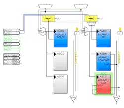
This circuit can be implemented with low-cost op amps, a multiple-channel two-input multiplexer (e.g., CD4053), a suitable ADC, and a few resistors. More easily, it drops into a Cypress PSoC1 part, such as the CY8C24423, which has the multiplexers, an instrumentation amplifier, and an ADC, either an incremental or a delta-sigma. The PSoC1 design requires no external parts. PSoC’s design tool, PSoC Designer, shows the implementation (Fig. 3).
The positive bridge output is connected to P0.1 for mux_1 and P0.0 for mux_2. The negative bridge output is connected to P0.7 for mux_0 and P0.0 for mux_1. The muxes are switched in software using the user modules’ standard application programming interfaces (APIs). It takes about 20 lines of C code to control the muxes and get data and a few more to display or send it. The instrumentation amplifier is brought out on P0.5 so you can see the amplified input toggling between its normal and inverting values.
To convince yourself that it works, short the inputs together at some mid-range value. Then, in software, average and stream out the VP value (the value of the differential amplifier’s input offset voltage) and the difference value. The ADCValueDiff is the offset-cancelled version.
Unless you got lucky and happened to pick op amps with super-low offset voltage, the difference will be clear. A quick test on four CY8C24423 chips showed that the instrumentation amplifier offset averaged 1.82 mV, which is well within the device spec. With the offset cancellation in place, the system offset was less than 6.0 μV. This is an offset reduction of a factor of 300, done with cheap parts and easy connections.
This circuit also works well with PSoC3, PSoC5, and PSoC4 series parts. The differential amplifier is constructed out of back-to-back programmable gain amplifiers (PGAs) in PSoC3 and PSoC5. PSoC4 requires resistors to set the gain in the differential amplifier. The differential amplifier outputs in these designs feed a differential ADC, eliminating the need for the third op amp in an instrument amp and a single-ended ADC.
Dennis Seguine is a member of the Technical Staff at Cypress Semiconductor Corp. He has been an applications engineer for Cypress Semiconductor since 2000, following many years of analog, embedded system, and software design for the underwater, instrumentation, and medical industries.


