This article is part of the Series: Ideas for Design: Ideas for Design Volume 2
This file type includes high resolution graphics and schematics.
Capacitive sensors are common in today’s consumer electronics, since they are used in many touchscreen applications. Most of the circuits for such applications are designed for small-area capacitors and finger contact operation.
This circuit is designed for large-area touch plates that can be activated at a distance and hidden behind walls or inside other structures. It uses the “driven shield” concept that was popular in the early days of audio engineering, when high-impedance sound sources such as crystal microphones were used. Shielded cables are needed to connect these devices, but the cable capacitance limits the high-frequency response.
The solution to this problem is to go back to the physics of a capacitor to find a way to reduce the cable capacitance. Driving a conductor between the outer shield and the inner, signal conductor with the same voltage as the signal conductor largely eliminates the capacitance. NASA used this driven-shield idea in a large-area capacitive sensor two decades ago (John M. Vranish, et al., US Patent No. 5,116,679).
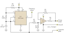
The circuit in Figure 1 performs the main capacitance-sensing task, while leaving detection to a microcontroller. IC1 is a 555 timer wired as an astable multivibrator with as small a timing capacitance as possible. With the component values shown, the frequency is slightly above 10 kHz. IC2 buffers the voltage on this capacitor to drive a shield plate.
For IC2, resistors R3 and R4 decrease the buffered voltage by about 1%. This prevents oscillation that may occur because of the external capacitance. R6 is included since some operational amplifiers have difficulty driving a capacitive load. IC2 should have a high gain-bandwidth product to allow a faithful representation of the signal voltage without phase shift.
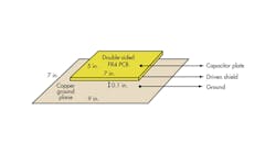
Figure 2 shows the construction of the sensing plate. These are the dimensions used in the author’s tests, but quite a lot of variation is permissible. A practical implementation would be to build the circuitry onto an edge of the ground plane.
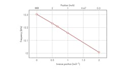
The frequency response decreases in a nearly linear fashion with respect to inverse position (Fig. 3). In the author’s test, hand contact reduced the frequency to 10.47 kHz. Hand contact through a 0.375-in. (10 mm) thick piece of plywood or gypsum wallboard resulted in a frequency change of 10%, which is easy to detect. Although frequency-detection ICs are available, a simpler, less expensive solution is to use a microcontroller to detect a change in signal period.
Dev Gualtieri received his PhD in solid-state science from Syracuse University in 1974. After many years doing research for a major aerospace company, he now does various computer, electronic, and embedded systems projects at his consulting company, Tikalon LLC. He also is the author of two science fiction novels, available on Amazon.


