More than 10 years ago, the frequency control industry introduced PLL-based (phase-locked loop) oscillators, an innovation that pioneered several features previously unavailable with traditional crystal oscillators (XOs). Leveraging internal clock synthesizer IC technology, PLL-based XOs can be programmed to support a wide range of frequencies.
This breakthrough eliminated the material processing steps required to cut and machine quartz to make it resonate at a particular frequency. It also made it possible for PLL-based XOs to be frequency-programmed and shipped to customers with very short lead times. Given that traditional oscillator lead times can approach 14 weeks or longer, many hardware designers rushed to take advantage of programmable oscillators due to their significant lead-time benefit.
This file type includes high resolution graphics and schematics when applicable.
Unfortunately, significant issues arose. Some designs that had migrated from using traditional XOs to using PLL-based XOs ran into jitter-related issues that caused application-related failures ranging from excessive bit-error rates in communication links to inoperable systems-on-chip (SoCs) and processors.
These issues forced many IC suppliers to specify that PLL-based oscillators could not be used in conjunction with their devices. This turn of events made it challenging for hardware designers to take advantage of the frequency flexibility and short lead benefits offered by PLL-based oscillators. So why did this happen? It turns out that PLL technology varies widely from supplier to supplier.
On The Bench
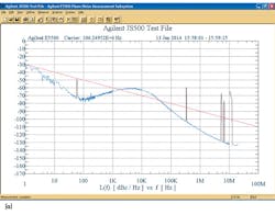
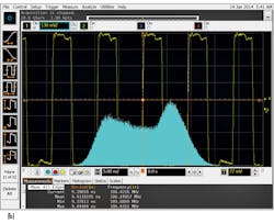
A sub-optimal PLL design leads to excessive oscillator phase noise and jitter peaking (Fig. 1a). The phase jitter of this particular PLL-based XO was measured at 150 ps RMS integrated over the 12-kHz to 20-MHz band. This level of performance makes it unsuitable for clocking high-speed physical layers (PHYs), which typically require <1-ps RMS jitter references. The bimodal period jitter may be a sign of a PLL stability issue that could have a detrimental performance impact on the SoC using this XO (Fig. 1b).
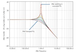
A second area of concern with programmable oscillators that exhibit jitter peaking is cascaded PLLs. When such a PLL-based oscillator is connected to an IC with a PLL in a subsequent circuit, jitter may increase. The good news is that not all PLLs, and certainly not all PLL-based oscillators, are created equal.
With proper PLL design techniques, programmable oscillators can deliver jitter performance rivaling best-in-class quartz oscillators while addressing the issue of cascaded PLLs. These high-performance PLL-based oscillators can be used for processor/SoC clocking as well as clocking high-speed serializers, PHYs, and FPGAs.
Developers can use three simple criteria to evaluate if a PLL-based XO can be used in a given application:
• Jitter generation: In cascaded PLL applications such as FPGA and PHY clocking, the XO reference clock jitter is compounded with the FPGA/PHY’s internal PLL jitter. Starting with a low-jitter XO reference (e.g. <<1-ps RMS phase jitter) maximizes the tolerable jitter that can be generated by the FPGA/PHY’s internal PLL, maximizing margin in the overall design.
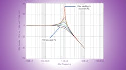
• Jitter peaking: Cascading PLLs run the risk of excessive jitter due to jitter peaking when the loop bandwidths of the first-stage and second-stage PLLs are the same. A PLL-based oscillator with a relatively low internal PLL bandwidth easily mitigates this risk. The PLL should be well damped to ensure less than 1% peaking (<0.1 dB), as shown in Figure 2. The bandwidth of second-stage PLLs in common SoC/FPGA devices is typically >1 MHz. Using a PLL-based oscillator with low jitter peaking and a much lower internal bandwidth ensures that its peaking won’t overlap with the downstream PLL’s bandwidth. This architecture enables the second-stage PLL to easily track changes in the first-stage PLL while maintaining acceptable loop stability and phase margin.
• Phase noise: How do you know if a PLL-based oscillator will work in your application? The oscillator period jitter can be observed easily using an oscilloscope. Oscillator phase noise can be measured using a spectrum analyzer. If you do not have access to a spectrum analyzer, contact your frequency control supplier for phase noise measurements. Phase jitter can be calculated directly from the phase noise plot by using the relevant jitter integration bandwidth required by the application. Phase noise plots also show the spurious performance of the reference clock. The spurious contribution to phase jitter can be measured easily to ensure the application’s requirements are met. The phase noise plot will also show any peaking effects of the internal PLL. Overdamped PLLs will exhibit low peaking.
Silicon Labs offers an easy-to-use online jitter calculator that converts phase noise to jitter. Simply input the carrier frequency and its associated phase noise profile, and the utility calculates the clock’s resulting phase jitter, period jitter, and cycle-cycle jitter. It is available at http://www.silabs.com/support/Pages/phase-noise-jitter-calculator.aspx.
What’s Next
Today’s programmable oscillators offer an excellent combination of frequency flexibility and short, reliable lead times. However, the underlying PLL performance offered by programmable oscillators can vary considerably from supplier to supplier. For high-performance applications including FPGA transceiver and Ethernet PHY clocking, programmable oscillators can be evaluated easily in terms of jitter generation by comparing datasheet specifications.
In applications where the oscillator is driving an ASIC, SoC, FPGA, or PHY with internal PLLs, it is important to ensure that the combination of the reference oscillator and the SoC does not generate jitter peaking, which typically is not specified in oscillator datasheets. An easy remedy is to take a phase noise measurement of the oscillator. This phase noise profile will show any peaking effects on the internal PLL and can be easily converted to provide the clock’s equivalent jitter performance.
James Wilson serves as marketing director for Silicon Labs’ timing products, overseeing the marketing program for the company’s clock and oscillator products. He joined Silicon Labs in 2002 as a product manager focusing on optical networking solutions. Previously, he worked at Freescale Semiconductor’s networking and communications systems group in Austin, Texas. He holds a BS in mechanical engineering and a master’s degree in business administration from the University of Texas at Austin. He can be reached at [email protected].


