Very-Low-Input-Bias-Current Op Amp Has Plenty of Written Support for Design Engineers
Download this article in .PDF format
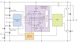
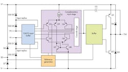
In a simplified schematic from its datasheet, Linear Technology's LTC6268 (and 6269 dual) provide no evidence of "secret sauce." Rather, it shows a combination of semiconductor design and process technology know-how leading to a number of remarkable specs, including an input bias current of only 3 fA at room-ambient temperature.
In other years, my choices for “best” analog products often focused on novel devices aimed at narrow application areas. This year’s main storyline, however, is about squeezing the latest in high performance out of the ubiquitous operational amplifier.
Late in September, Linear Technology announced single and dual FET-input op amps (LTC6268 and LTC6269) intended for application in wide-dynamic-range transimpedance amplifier (TIA) and buffer applications, mostly driving high-precision analog-to-digital converters (see the figure). The op amps’ key performance characteristic was that they drew a bare 3 fA of input bias current at 25°C (the complete bias current spec is 4 pA max over the entire –40 to +125°C temperature range). Resolving input currents that vary from a few femtoamps to multiple amps require “high” dynamic range.
Noise tolerance is also critical to achieve precision. In the two new LTC parts, the datasheets’ spec wideband voltage and current noise measured 4.3 nV/√Hz and 5.5 fA/√Hz, respectively. Other impressive performance characteristics include 500-MHz gain-bandwidth product, sub-picofarad input capacitance, and –100-dB harmonic distortion at 1 MHz.
Crucial Bias Current
Let’s take a look at that bias current specification. Why, and to whom, is that so important? In an ideal op amp, both the inverting and non-inverting inputs exhibit infinite impedance; no current flows into or out of them. In a real-world op amp, there’s always some current flow at both terminals. That’s a problem because those bias currents flow through the external circuitry connected to the inputs, which results in voltage drops that change the voltages seen at the op-amp inputs. In turn, measurement precision becomes diluted if the op amp is being used at the input of a test instrument, or it distorts the signal in other ways. And capacitively coupling the input doesn’t solve the problem.
Specs vs. Real Application Needs
What about the other specs? Where are the actual applications in which they hold significance? Linear says that it developed the parts for designers who need the topmost performance in photodiode and photomultiplier circuits, and similar high-impedance sensor applications. Perhaps its most ubiquitous application, though, will be matching driving performance to the highest precision analog-to-digital converters.
How’d They Do That?
It’s somewhat mind-boggling to consider the engineering that goes into creating a new analog component that manifests significantly enhanced specs. Companies that maintain a tradition of continually stretching the performance envelope are worth studying. I spoke with the lead designer on the project and tried to get some clues from the parts’ datasheet. There’s also a dedicated application note titled “Does Your Op Amp Oscillate?”.
The datasheet provides some clues about the challenges in designing the individual elements of the IC. It notes that “to minimize the LTC6268’s noise, its chip designers had to deal with input-referred voltage noise (eN), input-referred current noise (iN), and input capacitance (CIN).”
For a TIA application, the document explains, eN, iN, and CIN, in addition to feedback resistance RF, contribute to noise behavior in different ways. Meanwhile, external components and traces can affect CIN.
One thing you relearn again and again is that multiple causes impact every parameter. Input-referred voltage noise, for example, consists of flicker (1/f) noise, which dominates at lower frequencies, and thermal noise that affects higher frequencies. For the LTC6268 and 9, the 1/f corner, or transition between 1/f and thermal noise, happens at about 80 kHz.
Meanwhile, as the iN and RF contributions to input-referred noise current affect the minus input directly, the eN contribution is amplified by the device’s noise gain: (1 + 2π × RF × CIN × Frequency). That is, it’s affected by both the feedback resistor used by the circuit designer and the capacitance on the input, although all of this is limited by the closed-loop bandwidth. In general, the effects of eN dominate if CIN is “high” (~5 pF), and iN dominates when CIN is “low” (~1 pF). In other words, “Watch your layout on the circuit board that carries the part.”
Greater Depth in the App Note
The app note cited above has other accessible design information, too. It addresses the issue of self-oscillation, starting by showing open-loop gain and phase response plots versus frequency for the new op amps, and relating that to stability with feedback. Then it moves on to gain margin and its effect.
Next the note considers how the feedback network itself can induce oscillation, which is where readers can find some of the layout advice. The relevant paragraph begins: “Note that in Figure 4, [in the appnote] we have placed a parasitic capacitance in parallel with the feedback divider,” and continues “This is inevitable; each terminal of each component on a circuit board has about 0.5 pF to ground, plus that of the traces.
“In practice, nodes have a minimum capacitance of 2 pF, and ~2 pF per inch of trace.” [That makes it easy to] “rack up 5 pF of parasitic. Consider the LTC6268 providing a gain of +2. Attempting to save power, we set the values of RF and RG to a rather high 10 kΩ. With CPAR = 4 pF, the feedback network has a pole at 1/(2π × RF||RG × CPAR), or 8 MHz.”


