This file type includes high resolution graphics and schematics when applicable.
Despite the availability of FPGAs and microcontrollers, the historical use of analog circuitry to implement some arithmetic functions is still a viable and cost-effective technique. For the division of voltages, commonly used analog devices combine operational amplifiers with different multipliers for feedback.1 The maximum precision of the multiplier used is based on the accuracy of the transfer function of logarithmic and antilogarithmic functions of its diodes and transistors; the minimum error achievable using these multipliers is around ±0.1%.
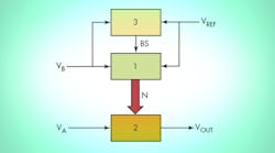
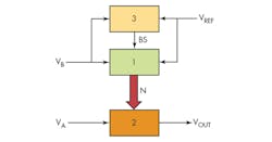
To achieve much greater precision, the proposed approach uses a modified analog-to-digital converter (ADC) and two digital-to-analog converters (DACs) to do the division, with the precision determined by the number of bits in each DAC. In the circuit structure of the division device (Fig. 1), Block 1 is an ADC with a special compensating circuit, consisting of an op amp with DAC1 as feedback. The ADC converts the voltage of the divisor to digital code N. Block 2 is another DAC (DAC2), which yields the output voltage resulting from the division. Block 3 is a comparator that interrupts the conversion if the divisor voltage drops below the minimum possible value.
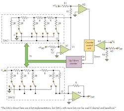
In the detailed example of a division circuit (Fig. 2), and using a simplification of realized dependencies, define N as:
N = Z/(Zmax + 1)
where Z and Zmax are present and maximum sums of least significant bits (LSBs).2 The sums of the LSBs depend on the code resolution.
The proposed ADC differs from the usual ADC implementation in its connection to DAC1, which provides feedback via its position between the input and output of amplifier A1.3 Output I2 of DAC1 connects to the input of A1, and output I1 connects to ground. The connection of amplifier A1 determines the feedback resistance as equal to R when N = 0. The equivalent resistance (DAC1) to output current I2 is R/(1 − N). The input resistor (R2) of amplifier A1 is 10R, when the reference-voltage source VREF is +10 V. The output voltage of amplifier A1 is:
V1 ∝ 1/(1 – N)
Input voltages VB of ADC and V1 connect to the comparator A2. With VREF = 10 V, the range of voltage VB is +1 V ≤ VB ≤ 10 V. The range of code N is 0 ≤ N ≤ 0.9 for the range VB. The ADC is balanced when VB – V1 = 0. Then,
V1 = VREF × 1/[10(1 – N)] or (1 – N) = VREF/10VB
The output section consists of DAC2 and amplifier A4. DAC2 connects to the input of amplifier A4 by output current I2. Therefore, code N is the information component of VB only.
VOUT = ±VA(1 – N), or VOUT = ±VA × VREF/10VB
The third part of the device is the comparator A3, which creates a blocking signal BS for controlling the counter. Voltage VB is compared with VREF × [R4/(R3 + R4)]. If VB becomes less than 1.0 V, then the output signal BS of A3 changes to stop the counter. The output voltage of the division circuit changes polarity depending on the polarity of VA.
This file type includes high resolution graphics and schematics when applicable.
The example circuit provided here reduces the error to less than ± 0.02%, based on the resolution of both DACs. You can increase precision further by increasing the number of bits, with the resistors connected in series within each DAC.
References:
1. Ulrich Tietze, Christoph Schenk, & Eberhard Gamm; Electronic Circuits, 2nd ed., Springer 2008, p. 762.
2. Ibid, p. 960.
3. Ibid, p. 953.


