Digitally Programmable Amplifier Meets Sensor Gain, Ranging Needs
This file type includes high-resolution graphics and schematics when applicable.
Most data-acquisition systems with wide dynamic range need a method of adjusting the input-signal level to the analog-to-digital converter (ADC) to ensure the maximum input signal will be fairly near to the ADC's full-scale input voltage (note that a typical ADC's full-scale input-voltage range is between 1 V and 10 V). At the same time, the gain applied to a sensor output may also need to be adjusted during run time, for example, to compensate the nonlinear output across the temperature range. To achieve this, a programmable gain amplifier (PGA) or a variable gain amplifier (VGA) is usually located between a sensor and its ADC (Fig. 1).
Both PGAs and VGAs usually allow for selection of fixed gains whose values are typically between 1 and 100. Some applications, such as sensing and/or controlling current flow, require applying specific gains to optimize both the sensor output-voltage range and the ADC’s resolution. In these cases, the required gains can vary between 1 and 1500 or more, and its values don’t fit to the selectable values in commercial PGAs or VGAs.
When choosing the topology of the amplifier circuit with a very high gain, it’s convenient to bear in mind that in many cases, it’s not advisable to use feedback resistors with a very high value (> 1 Mâ¦) due to the present noise. In addition, if it’s necessary to implement an amplifier with a very precise gain, then the current by the resistances must be much greater than the op amp’s offset current. This is only possible if the resistors don’t have a very high value. On the other hand, it’s always necessary (desirable) that the amplifier input resistance be reasonably high (not very small).
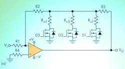
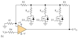
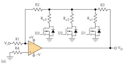
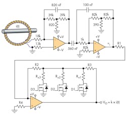
Figure 2 shows two amplifier circuits with eight digitally programmable gains that meet all of the above conditions. Although the number of gains that can be implemented with these circuits is equal to 2n, where n equals the number of MOSFETs, it’s only possible to implement n independent gains. The values of the implemented gains in these circuits are easily adaptable to the needs of virtually any application that’s considered.
Figure 2a represents an inverting amplifier circuit, while Figure 2b is non-inverting. In both circuits, digital signals D1, D2, and D3 are used to select the gain of the amplifier. The MOSFETs used must be logic-level MOSFETs (or logic-level gate MOSFETs) with an RDS(ON) as low as possible (such as the 2N7002P with typical RDS(ON) = 1 Ω or the IRLML2502 with a typical RDS(ON) = 0.05 Ω).
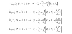
The independent gains that can be selected in the amplifier circuit of Figure 2a are:
When two or more MOSFETs are used, the body diode of a MOSFET will start to conduct current if the input voltage (vi) becomes too large, thus distorting the amplifier’s output voltage. To avoid this, the following condition must be satisfied:
where vF is the body-diode forward voltage of the MOSFET (vF > 0).
When only one MOSFET is used, the input voltage must fulfill the following condition to avoid body-diode conduction:
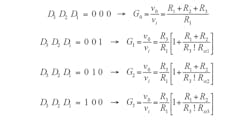
The independent gains that can be selected in the amplifier circuit of Figure 2b are:
In the circuit of Figure 2b, when using two or more MOSFETs, the body diode will conduct current if the input voltage (vi) takes too small negative values, distorting the output voltage of the amplifier. To avoid this, the following condition must be satisfied:
When only one MOSFET is used, the input voltage must fulfill the following condition to avoid body-diode conduction:
Figure 3 shows a practical application of the circuit of Figure 2a. In this example, a controllable-gain amplifier is used to amplify the output voltage (vi) of a circuit that integrates and filters the signal generated by a Rogowski coil. Assume the ADC that will sample the signal vo = k × i(t) has reference voltages of vREF+ = 2.5 V and vREF - = –2.5 V, the Rogowski coil has a sensitivity constant of 30 μV/A, the integrator high-pass filter has a voltage gain of 1.2 (1.64 dB) at 50 Hz, and we want to measure ac currents in the following ranges: 1280, 320, 80, and 20 ARMS.
The gains to select are: G0 = –38.363, G1 = –153.452, G2 = –613.808, and G3 = –2455.2. Many combinations of the resistances in the circuit shown in Figure 2a can provide these gains. The following offers a simple and fast method to calculate the appropriate values of the resistors:
Rα3 = 300 × RDS(ON) = 300 × 1 Ω = 300 Ω, so we set the smallest value of the Rα resistors to ensure that the value of RDS(ON) doesn’t have a significant influence on the amplifier gains.
The gains obtained with the calculated values are (theoretical values are shown in square brackets):
In the case of using the amplifier circuit shown in Figure 2b, the following method can be used to determine the appropriate values of resistors that provide gains G0 = 38’363, G1 = 153’452, G2 = 613’808 and G3 = 2455’2:
R1 = 4 · Rα3(G3 – G0)/(–1 +G20) = 1972 â¦
The gains obtained with the calculated values are (theoretical values are shown in square brackets):
Carlos Castro-Miguens received his Electronic Engineering degree from Vigo University, Spain. He is currently employed as associate professor of the Electronic department at Vigo University. His primary interests are in power electronics (dynamic modelling and control of power converters, design of magnetic components for power converters) and design of embedded systems. He can be reached at [email protected]
Jose B. Castro-Miguens received the Electrical & Electronic Engineering degree from UPCO University, Madrid, Spain, in 2003. He is currently employed (since 2003) by the Cesinel Company, working as design engineer on power electronics, instrumentation engineering, signal processing, and electric power control.
