Download this article in .PDF format
Protecting users from potentially lethal voltages and currents is a key requirement in any electrical design. The latest generation of reinforced-isolated devices is allowing designers to replace two separate levels of protection with a single component that performs the equivalent function. This article will discuss the semiconductor technology that enables this advance and the tests that ensure user safety isn’t compromised.
The Need for Isolation
An isolation device prevents the propagation of dc and unwanted ac currents between its input and output while allowing the transmission of the desired signal. It accomplishes this using an isolation barrier that has a high breakdown voltage and low leakage. No resistive path exists across the barrier, but the device can still transfer information across it by capacitive, inductive, or optical techniques.
Isolation is useful in non-safety-related situations, too. For example, ground reference levels can vary widely between two separate electrical systems, such as different parts of an industrial plant.
Such differences can cause errors or failure in a digital transmission; any difference in grounds between transmitter and receiver reduces the margin for error. In an analog circuit, any dc ground difference between devices adds an unwanted offset error; an ac variation can affect the harmonic content of the signal. Adding an isolation device to a circuit can correct for ground differences.
In some applications, a low-level signal of interest may ride on a larger common-mode (CM) voltage that appears simultaneously on both input terminals. The combined signal can be greater than the full-scale range of a downstream device or exceed its overvoltage limits and cause damage. An isolation device is able to block the common-mode voltage and make sure that only the signal to be measured passes across the isolation barrier.
Regulatory Standards
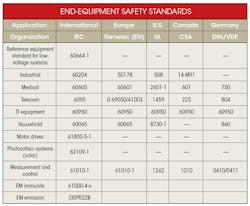
Although isolation devices fulfill several different functions, their safety performance is the primary concern of the regulatory agencies. Figure 1 shows some of the regulatory standards that set safety standards for various applications. There are different regulations for components and end equipment. In addition, separate standards exist for optical and magnetic isolation technologies.
Common Isolation Terms
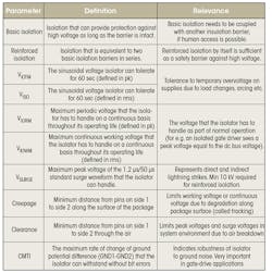
To understand the regulations let’s review some basic definitions. Figure 2 shows the definitions of the isolation specifications in a typical datasheet.
Functional isolation is sufficient for proper system operation, but doesn’t necessarily provide a barrier against shock. An isolation device that’s only used to break a ground loop in a low-voltage design, for example, doesn’t need to provide shock protection.
Basic isolation provides protection against electric shock as long as the barrier is intact. However, when human access is a possibility, safety regulations require double isolation with a second level of protection, such as supplementary insulation or protective grounding.
To provide this required protection while reducing cost and size, reinforced isolation defines a single level of isolation that provides shock protection, isolation, and reliability equivalent to two levels of basic isolation.
Requirements for Reinforced Isolation
How do reinforced-isolation devices ensure safety? VDE 0884-10 (soon to be “-11” with additional required tests) is the most demanding worldwide standard for reinforced-isolation components. Although VDE 0884 strictly applies to isolators that use capacitive isolation technology, it’s more demanding than IEC 60747-5-5, the equivalent standard for optocouplers.
VDE 0884-10 specifies a rigorous series of tests for isolation components. Test procedures are different for basic and reinforced isolators, and more stringent for reinforced devices.
The parameters tested are defined in Figure 2. They include the maximum repetitive peak voltage (VIORM), working voltage (VIOWM), the maximum transient isolation voltage (VIOTM), isolation withstand voltage (VISO), maximum surge isolation voltage (VIOSM), and the comparative tracking index (CTI). These specifications represent the isolator’s capability to handle high-voltage stresses of different magnitudes and transient profiles, and have a direct correlation to real-world operation.
VIORM and VIOWM, for example, both measure the ability of an isolator to withstand high voltage across its barrier on a continuous, day-to-day basis throughout its lifetime.
VDE 0884-10 checks for VIORM and VIOWM through a partial discharge test that detects localized discharges inside the insulation, indicating degradation in the insulation. The partial discharge test is performed along with the test for VIOTM. There are different tests for certification and during production, referred to in VDE 0884-10 as Test Method A and Test Method B1, respectively. During certification, multiple devices are tested from different wafer lots; during production, 100% of devices are tested.
Reliability Calculations for Isolation Devices
To verify the long-term reliability of an isolation device, the manufacturer must provide accelerated-stress test data to the certifying agencies. During an accelerated-stress test, the isolator is subjected to varying voltage levels that considerably exceed its working voltage. The corresponding times to breakdown are recorded and the voltage-versus-time curve is extrapolated to predict the lifetime at the expected working voltage.
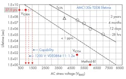
The Time Dependent Dielectric Breakdown (TDDB) test, the industry-standard method used to verify the dielectric lifetime, is a key test of the HV isolation barrier. The TDDB test stresses parts at a constant high ac or dc voltage for an extended period until the insulator wears out and fails by electrical short. By testing TDDB at multiple voltages, the product lifetime at the working voltage is determined by extrapolation (Fig. 3).
VDE 0884 specifies the margins required to establish the lifetime of a capacitive reinforced-isolation part. These include a 20% margin in working voltage and an 87.5% margin in operating life; for example, a device rated at 1-kVRMS working voltage with a lifetime of 20 years must demonstrate a probability of failure of less than 1 ppm for operation at 1.2 kVRMS over 37.5 years.
Overview Of SiO2 Capacitive Isolation Technology
How does the construction of an isolation device enable it to meet these agency requirements?
Capacitive isolators primarily use high-voltage silicon-dioxide (SiO2) capacitors to provide isolation. With a dielectric strength of 470-670 V/µm, SiO2 has the highest dielectric strength among HV isolation materials commonly used. Unlike polyimide and other polymer-based insulators, SiO2 is free of voids and the reliability of a SiO2 capacitor doesn’t degrade with exposure to ambient moisture.
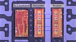
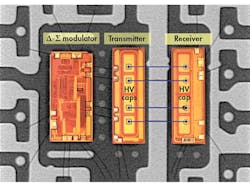
Reinforced isolation is achieved using two thick SiO2 capacitors in series between input and output that constitute a double isolation barrier. The HV capacitors are manufactured in a high-performance analog CMOS process and packaged in a multi-chip SOIC module (Fig. 4).
The wafer fab process is a multilevel metal process, with the HV capacitor formed between metals. This structure achieves the SiO2 thickness needed for HV isolation using standard inter-level dielectric layers. The multilayered structure improves quality and reliability by reducing the dependence of the HV performance on any single layer.
For SiO2-based isolators, the relationship between time-to-failure and stress voltage follows an exponential curve. Consequently, the log of expected time-to-failure reduces linearly with voltage stress applied, and VDE 0884-10 requires SiO2-based isolators to use this same relation to curve-fit accelerated test data.
Examples of Reinforced-Isolation Devices
TI’s AMC130x is the first product family that combines analog operation with a reinforced-isolation rating. It provides reliability, shock protection, and isolation corresponding to two levels of basic isolation in a single package.
Devices in the family provide reinforced-isolation options for common data-acquisition functions. They deliver isolation of up to 7 kVPEAK with a working breakdown voltage of 1 kVRMS. Insulation barrier lifetime is 64 years, in excess of the requirements of VDE0884-10.
The AMC1305, shown in Fig. 4, is a precision delta-sigma (ΔΣ) modulator with 16-bit resolution and either an LVDS or CMOS digital interface. The AMC1304 is a similar device, but also includes a low-dropout regulator (LDO).
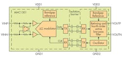
Figure 5 shows another family member, the AMC1301. It uses the ΔΣ modulator as the basis of a precision isolated operational amplifier.
For digital applications, TI offers the ISO784x and ISO782x families of reinforced isolators. They come in two- and four-channel versions with data rates up to 100 Mb/s.
Conclusion
The HV performance of a capacitive reinforced-isolation device is quantified with different parameters, which represent the isolator’s capability to handle high voltage stresses of different magnitudes and transient profiles. Safety agency VDE issues the VDE0884 component-level standard that defines these parameters and the methodologies to test them.
Texas Instruments has developed multiple isolators with reinforced-isolation capability that meet or exceed these stringent requirements.
