Fast ADC Facilitates Direct RF Sampling at Higher Frequencies
Download this article in PDF format.
The critical component in all digital communications receivers is the analog-to-digital converter (ADC). The ADC sampling rate, bandwidth, and noise tolerance establishes the specifications and performance of the receiver. However, receiver architecture also plays a major role in its performance. An architecture that significantly improves performance over previous designs is direct RF sampling—and it’s become more practical than ever thanks to the availability of fast wideband ADCs.
Receiver Architecture Review
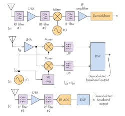
Perhaps the most widely used receiver architecture is the superheterodyne, where the received signal is downconverted to a lower intermediate frequency (IF) by a mixer before filtering and demodulation. In a typical arrangement (see the figure, a), the bandpass filter (BPF) narrows the bandwidth and the low noise amplifier (LNA) boosts the signal level. The local-oscillator (LO) frequency mixes with the incoming signal to produce a lower IF. The signal modulation, bandwidth, and data are retained. A demodulator recovers the original data.
One major disadvantage of the superhet is that it uses many circuits and filters, increasing the cost. In addition, the local oscillator (LO), often a PLL synthesizer, adds phase noise and jitter. Perhaps the biggest downside is that the mixing process generates images that can cause interference to the signals being received. Some designs are dual- or triple-conversion types, where two or three downconversions (or an upconversion in some cases) are used to provide image rejection.
1. The classical superheterodyne receiver architecture is still widely used but has some disadvantages at the very high frequencies (e.g., images are a perpetual problem) (a). The direct conversion receiver mixes the incoming signal with a local oscillator of the same frequency, resulting in the direct recovery of the baseband data being transmitted (b). The direct RF sampling receiver architecture is simple and offers multiple advantages at VHF, UHF, and microwave frequencies (c).
Microwave and millimeter-wave signals in the 1- to 300-GHz range are routinely mixed down to an IF in the 70- to 500-MHz range. That’s been done primarily due to the speed limitations of available ADCs and fast DSP processors. However, the availability of faster ADCs and DSP/FPGAs is changing that scenario.
Another popular architecture is the direct conversion receiver (see the figure, b). The LO frequency is equal to the incoming signal frequency, and the mixing of the two produces an intermediate frequency of zero. This zero IF architecture downconverts the RF signal directly to baseband. The positive result is less circuitry, lower cost, and complexity, and a more accommodating ADC sampling rate. No images are generated, but the zero IF receiver presents a dc offset problem and LO leakage to the input. Nonetheless, it is widely used.
A receiver architecture that’s gaining in popularity is direct RF sampling. RF sampling is the process of directly digitizing the received signal with no downconversion (see the figure, c). Some filtering and RF amplification typically occurs prior to the ADC. For this to work, the ADC must be fast enough to sample the input signal within the Nyquist limits of the device. A sampling rate of at least 2.5 times the highest frequency content is required. A common minimum sampling rate is greater than twice the bandwidth of the signal to be received, otherwise known as oversampling. Oversampling offers the benefit of reducing the quantization noise produced by the sampling process. This greatly improves the signal-to-noise ratio (SNR).
Benefits of RF Sampling
The simpler receiver signal chain offers some significant benefits. Fewer stages generally mean lower cost and better noise figure. Higher RF gain may be needed to offset the gain of the mixer and any IF amplifier, but the overall noise figure will be improved. An image problem does not exist.
The local-oscillator feedthrough and spur issues are also vanquished. It eliminates a local oscillator, but is essentially replaced by the ADC sampling clock. This architecture typically offers greater flexibility for frequency planning in design, a modern necessity because of the wide range of potential interference sources and targets.
Applications
A super-fast ADC potentially opens up a lot of application doors, particularly in RF communications. Some examples are software-defined radios (SDRs) of all types, satellite communications, radar, communications test equipment, forthcoming 5G radios, and digital sampling oscilloscopes.
Fast ADCs can be a major benefit in electronic-warfare (EW) equipment, where the core component is one or more receivers in radars, military radios, and signal-intelligence devices. For example, expect major performance strides to be made in phased-array radars, where each antenna element in the array has its own receiver chain and ADC. Wide-bandwidth receivers let radars detect and process more targets, ultimately providing an advantage over the enemy. Another forthcoming use is large-scale MIMO systems for cellular basestations.
An Example ADC
Typical of the fast new ADCs is Texas Instruments’ ADC12DJ3200, a dual-channel 12-bit converter. It offers a sampling rate of 3.2 Gsamples/s per channel or 6.4 Gsamples/s in an interleaved single-channel application. The differential analog inputs are buffered and the −3-dB bandwidth is an impressive 8 GHz. This makes the device suitable for use with L-, S-, and C-band radar, in addition to other applications. Another key feature is a noise floor in the −151.8- to −154.6-dBFS/Hz range. Some other important specs are a signal-to-noise ratio (SNR) of 56.6 dB and a spurious-free dynamic range (SFDR) of 67 dB. The ADC outputs are JESD204B serial data interfaces with a maximum lane rate of 12.8 Gb/s.
Dual digital downconverters (DDCs) are also included on-chip. Four 32-bit numerical-controlled oscillators allow decimation by 2x, 4x, 8x, or 16x. Decimation removes samples from the ADC output at regular intervals to decrease the sample rate so that the data can be accommodated by the processing circuits.
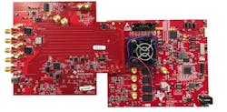
2. The TIDA-01442 reference design implements and demonstrates a direct RF-sampling receiver for a radar receiver operating in HF, VHF, UHF, L-, S-, C-, and part of X-band.
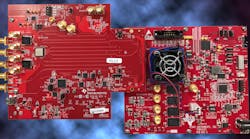
To evaluate the capabilities of the ADC12DJ3200, Texas Instruments offers the TIDA-01442 reference design that uses the ADC12DJ3200 evaluation module (EVM) (Fig. 2). It demonstrates a direct RF-sampling receiver for a radar receiver operating in HF, VHF, UHF, L-, S-, C-, and part of the X-band. The wide analog input bandwidth and high sampling rate (6.4 Gsamples/s) of the ADC provide multiband coverage with a single or dual ADC. The direct RF-sampling capabilities of the ADC reduce the component count by eliminating several downconversion stages, thereby reducing overall system complexity.
Clocking Considerations
High-speed multichannel ADC applications require precise clocking solutions capable of managing channel-to-channel skew to achieve optimal system SNR, SFDR, and ENOB. That makes the clock for the ADC a critical component if the desired benefits are to be achieved. TI offers the solution in the form of its LMX2594, a wideband RF phase-locked-loop (PLL) IC with integrated VCO.
This PLL supports both fractional-N and integer-N modes, and provides an on-chip 32-bit fractional divider that permits fine frequency tuning of clock frequency. This IC offers critical specifications such as −110-dBc/Hz phase noise at 100-kHz offset with a jitter of 45 fs rms at 7.5 GHz. Support is provided for a JESD204B interface and SYDREF.
TI also offers a reference design for this device. Designated the TIDA-01021, the reference design uses the ADC12DJ3200 ADC evaluation module. It supports two high-speed channels on separate boards by using the LMX2594 wideband PLL. Representative performance indicates a board-to-board clock skew of <10 ps with an SNR of 49.6 dB using a 5.25-GHz input signal.


