Constant-Current APD Bias Method Automatically Optimizes Optical Comms Performance
Download this article in PDF format.
An avalanche photodiode (APD) delivers a useful electron-multiplier gain and generally improves signal-to-noise ratio (SNR) in optical communication systems. An APD is similar to a PIN photodiode with the addition of a thin, high electric field region next to the depletion region where photons generate electron-hole pairs. Photo-generated carriers rapidly drift into the high field region and acquire energy from the applied field.
When photo-generated carriers receive sufficient energy, they knock other electrons out of the semiconductor lattice to create secondary electron-hole carrier pairs. The secondary carriers in turn receive energy from the applied electric field and create additional carriers as they all drift through the thin, high electric field region. The process continues until the carriers pass out of the high field region.
Avalanche multiplier gain is nonlinearly proportional to the bias potential voltage applied to the APD. Gain increases to hundreds or thousands as bias potential approaches reverse breakdown, where an APD behaves like a Zener diode.
There is a large field of study1,2 regarding gain and noise mechanisms of various APD structures. Noise increases rapidly at higher avalanche gain, so there will always be an optimum gain and bias setting, depending on many parameters. For our purposes here, it’s sufficient to say that APD gain isn’t noise-free and does degrade the SNR as it appears at the input to the photodiode.
However, Johnson (resistor) noise in the following preamplifier dominates the noise out of PIN photodiode detectors by perhaps 100 times, so any avalanche gain initially improves performance no matter how noisy the APD. Silicon APDs generally have much lower noise than III-V APDs and deliver very much more usable gain.
Substitution of an APD for a PIN photodiode significantly boosts performance, but there are constraints and penalties.
Below optimal gain, performance is less than it can be. Above optimal gain, APDs generate a lot of noise that rapidly degrades performance.
During bit-error-rate (BER) measurements on communication systems in the laboratory, one sees a relatively narrow minimum in errors as the bias potential varies through optimum. Optimal bias potential may vary widely among device samples; therefore, users must measure and determine the optimum bias potential for each sample individually. Avalanche photodiode characteristics also vary with temperature, so bias compensation schemes measure and accommodate temperature changes as well.
Ever since their introduction, users have tried to harness the benefits of APDs while attempting to control bias potential over the narrow range that yields these benefits. RCA in Vaudreuil (then GE, then EG&G, then Perkin-Elmer, and now Excelitas) provides silicon APD devices like the C30919E with circuitry to control bias versus temperature with adjustable slope and intercept.
Constant-Current Bias
Operation of the APD at constant-current bias offers several advantages and a serious drawback when accommodating large signals. Consider an APD biased with a constant current. In the dark, bias potential across the APD rises to breakdown as in a Zener reference diode. Current flow is due only to multiplied thermally generated dark current and is all noise.
With illumination, there’s a signal photocurrent. Bias voltage falls below the breakdown potential. Gain decreases to a value equal to the APD current divided by the signal photocurrent plus the dark current. Output current initiated by modulated data supplants Zener current that’s due to multiplied dark current.
With increasing illumination, APD bias continues to fall and SNR continues to improve.
I force the APD current to the level that yields optimal performance at the lowest signal condition that meets the system requirements for BER. When the input optical signal reaches that level, the optimum bias appears across the APD, so it operates at optimal gain. While the optimal bias varies among APD device samples and over temperature, the optimal current varies little. I use this characteristic to control the applied bias. My arrangement automatically accommodates changes in temperature and input light level. Operation at the low end of the signal level range is automatic. I force the desired minimum signal current to flow through the APD.
With increasing signal level, the bias automatically adjusts to still lower gain to maintain the constant current. The performance improves from the minimum signal case because gain and noise are lower. Though the actual optimum may be at slightly different gain, the difference in bit-error rate isn’t readily measurable because the error rate is already so low.
It turns out that while the optimum voltage varies widely from sample to sample and over temperature, the signal photocurrent through the APD is always close to the same value. This value depends primarily on the particular type of APD, the particular preamplifier that follows the APD, and the bandwidth of that combination or any following band-limiting filter. Thus, it makes sense to determine the optimum current for that particular system, and then control to that optimum current and allow the system to vary the bias potential accordingly, rather than try to control the bias potential in the first place.
Dynamic Range
The constant-current bias approach fails at high signal levels. Increasing signal level decreases APD bias potential. At some point, the bias potential will drop below a value needed to sustain operation. This occurs for different reasons among different device types, but no APD will operate below some minimum bias potential.
The lower the value of the constant current chosen, the less dynamic range the constant-current approach accommodates.
To be really useful, we must be able to replace a PIN photodiode with an APD and still accommodate the largest optical signal that the PIN photodiode can handle. This is a real requirement if you don’t want to install variable optical attenuators throughout your fiber network or otherwise guarantee signal level won’t rise to too high a level.
Hybrid Method of Constant-Current Bias with Minimum Voltage Clamp
1. A diode combines constant current and constant minimum voltage sources to bias an APD.
A simple fix retains the advantages of constant-current operation at low level and still accommodates a large dynamic range of input signal. The constant-current approach works to the point where the input signal is so large that it forces the bias potential down to a threshold where the APD ceases to work. Somewhat above this point, simply clamp the APD bias potential to a minimum value and allow photocurrent to increase. Figure 1 illustrates the concept.
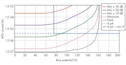
Figure 2 shows a load-line for this hybrid method in blue superimposed on the current versus voltage characteristic curves of a sample APD. The characteristic curves illustrate the behavior of the APD in the dark, with the smallest input optical signal that will yield 10-12 BER, and with signal levels 10, 20, and 30 dB greater than that level. The load line forces constant-current operation from the reverse breakdown potential down to 75 V. All available sample devices continued to operate normally down to 75 V bias.
2. The plot shows APD current versus bias potential with optical signal level as a parameter, and displays constant current and constant minimum voltage regions.
Constraints
This method works well within the following constraints:
- Constraint 1: There must be no extraneous input optical signal as one would encounter with background radiation in a free-space optical communication link. All of the signal must come from the desired source. Fiber optics is eminently well-suited.
- Constraint 2: The signal must be continuous rather than occur in bursts. Many high-speed data-communication protocols transmit characters continuously to maintain synchronization and meet this requirement. Failure to meet this requirement results in the start of the message undergoing excessive gain until it eventually decreases to the correct level.
- Constraint 3: The APD must not have a reach-through structure. There are basically two types of APDs. In one type, avalanche gain decreases with decreasing bias down to where the device acts as a PIN photodiode. At some point, the fields within such a device will become so low that the device’s speed degrades below what the system requires to function, but high speed is desirable down to unity gain. In the other type, the device ceases to function below a certain bias potential even while still at high avalanche multiplier gain. This type typically has a reach-through structure and isn’t suitable in this constant-current method of operation, even though reach-through APDs often have better noise performance.
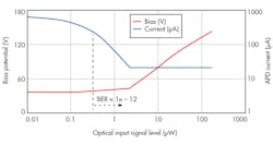
Figure 3 shows the behavior of the device under test biased with the approach shown. The bias was a constant 4 mA for optimal sensitivity and limited to a minimum potential of 80 V. BER fell below 10-12 at –35.5 dBm or about 300 nW and never came up again over the whole dynamic range. Subsequent measurements had slightly better optimums at slightly lower currents.
3. This plot of APD current and voltage versus input signal power shows current increases as bias approaches Vmin.
The test devices were Pacific Silicon Sensors part number AD230-2.3G-TO53 silicon APDs with integrated transimpedance preamplifiers.
Note that APD bias current is not absolutely constant on a short time scale comparable to the bit time, but over a much longer period due to the bias filter. A truly constant current that follows the ones and zeroes in the data would eliminate any modulation.
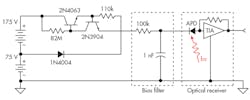
Figure 4 shows a simple circuit that implements constant-current control with a minimum clamp potential.
4. The circuit shows a simple version of the hybrid bias method for constant current with minimum voltage.
Present Status
The author performed this work in 2001. The USPTO granted patent number 6,654,215 in November 2003 to the Boeing Company. This patent expired in 2011 for non-payment of fees.
To my knowledge, no one ever used this powerful method. Now that patent protection has lapsed and this information is in the public domain, I hope someone will.
Sam Green retired as a technical fellow from McDonnell Douglas/Boeing after 42 years in 2011. Sam has undergraduate and graduate degrees in Electronic Engineering from Northwestern University in Evanston and the University of Illinois at Urbana respectively. Sam specialized in optical data communications and photonics. Sam is a life-senior-member of IEEE, a Registered Professional Engineer in Missouri, and an extra class radio amateur. Sam has dozens of publications and holds eighteen patents. Contact Sam at [email protected].
References:
1. McIntyre R.J., "Multiplication Noise in Uniform Avalanche Diodes," IEEE Transaction on Electron Devices, ED-13(1),164-168 (1966).
2. Webb P.P., McIntyre R.J., Conradi J., "Properties of Avalanche photodiodes," RCA Review (1974).


