The most common method for sharing data between devices is via a digital means of communications. Several standard buses implement such methods, with the main differences between them being data rate and noise sensitivity. When it comes to industrial applications or high-noise environments, communications systems suffer from noise interference. Thus, differential buses are often the best option as a result of their significantly reduced sensitivity to noise.
RS-485, also known as TIA-485(-A) or EIA-485, is a standard defined by the Telecommunications Industry Association and Electronic Industries Alliance (TIA/EIA). It’s based on balanced electrical signaling (a differential bus) that can be used effectively over long distances and in electrically noisy environments such as industrial environments.
RS-422, also known as TIA/EIA-422, specifies electrical characteristics of a digital balanced signaling circuit. This bus is very similar to RS-485, with the main difference being that the RS-485 can implement linear bus topologies with only a twisted pair of cables.
These buses are commonly used with embedded systems that implement half-duplex asynchronous serial communications. To do this, a conversion from single-ended buses to differential buses must be used.
Several different brands of commercial ICs implement the single-ended to differential bus conversion. These offer a simple way to convert RS-232-compatible buses to RS-422/RS-485 bus. Such ICs are called RS-422/RS-485 transceivers.
In this article, the required digital logic to implement an integrated transceiver for RS-422/RS-485 protocols converting single-ended to differential data when transmitting, or differential to single-ended data when receiving—managed by control signals—is used. To achieve this, we (at ADOM Ingieneria) used a Dialog Semiconductor GreenPAK SLG46533.
The system has two differential input/outputs as the interface to the RS-422/RS-485 bus—one control signal for flow data control and one serial data input (Tx to the bus) and one serial data output (Rx from the bus) as the interface to the singe-ended bus. With this implementation, the SLG46533V will work as a transceiver and is able to replace commercial ICs.
Differential Communications
Two basic forms of data-transmission circuits exist on serial communication buses: a single-ended bus and differential bus.
1. Single-ended or unbalanced circuit.
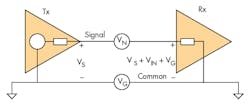
A single-ended or unbalanced circuit (Fig. 1) determines the bus state through the voltage difference between the signal line and common local ground. Fig. 1 shows the electrical schematic diagram of a single-ended transmission circuit, as well as the noise sources VN and VG. Noise voltages are added directly to the signal voltage (VS).
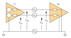
A differential or balanced circuit is shown in Figure 2. In this case, the bus state is determined by the voltage difference between two complementary signal lines. Fig. 2 illustrates the electrical schematic diagram of a single-ended transmission circuit and the noise sources VN and VG. Noise voltages VN and VG are added to each signal line and are common to both signals.
2. Differential or balanced circuit.
In this case, input voltages to the receiver stage are calculated with the equations:
VIA = VSA + VN + VG
VIB = VSB + VN + VG
The differential receiver measures the difference between the two lines. The received signal voltage is calculated as follows:
VRX = VIB – VIA = VSB − VSA
From Fig. 1, it can be seen that single-ended buses are susceptible to external noise influences. Also, due to the lack of any complementary signal presence, the electromagnetic fields created by the single-ended signal aren’t canceled, so it radiates much more noise than differential circuits. Electromagnetic-noise susceptibility and emissions relegate single-ended interfaces to low signaling rates and short transmission lines.
It can be seen that the differential receiver rejects the common voltage of the signals. If this bus type is used with closely coupled lines, the complementary signals cancel each other’s noise, resulting in high immunity and low noise emissions.
This immunity to external noise influence is the main reason for choosing differential signaling when relatively high signaling rates and long distance are required in electrically noisy, or noise-sensitive, applications. The disadvantage of differential buses is the additional cost of the line driver, receiver, and interconnection, versus the cost of single-ended transmission buses.
RS-422/RS-485 Bus
As mentioned, RS-422 and RS-485 are very similar differential bus standards. The first published standard was RS-422. But it lacked bidirectional capabilities allowing for multipoint connections, which led to the creation of RS-485.
RS-485—or TIA-485(-A) or EIA-485—defines the electrical characteristics of the interconnection, including driver, line, and receiver. It allows data rates up to 35 Mb/s and line lengths of up to 1200 m. As to be expected, both limits can’t be reached at the same time. There are several recommendations about wiring and termination; the standard doesn’t specify the connector or any protocol requirements.
A half-duplex and differential transmission method defined by RS-485 is designed for twisted-pair cables and other balanced media. The standard requires drivers to deliver a minimum differential output voltage of 1.5 V with up to 32 unit loads of about 12-kΩ each, plus termination resistors at each end of the bus.
Unlike RS-422 with its single driver circuit that can’t be switched off, RS-485 drivers use three-state logic that enables deactivation of individual transmitters. This allows RS-485 to implement multipoint linear bus topologies using only two wires. The linear bus topology is often based in a master-slave arrangement, where one device (the master device) initiates all communication activity.
As mentioned earlier, due to its differential transmission form, RS-485 is very robust against electrical noise. Due to its wide common-mode voltage range, it’s tolerant to ground potential shifts between nodes. These two characteristics are the main reasons for using RS-485 in applications that require low noise emissions and susceptibility.
3. RS-485 network schematic.
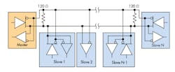
In most applications, the signaling rate and long distance lines are sufficient to control a process line or share data in industrial environments. Figure 3 shows an RS-485 network schematic.
The RS-485 standard doesn’t define particular protocols for communications with the bus; it only specifies electrical characteristics of the interconnection. Thus, RS-485 is used with many communication protocols as the physical layer of the communication system.
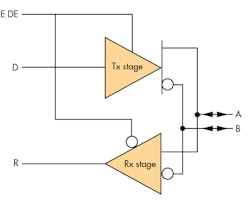
Due to the differential nature of the RS-485 bus, transceivers are used to convert single-ended buses to differential versions. That’s because typical communications systems or microcontroller serial communications peripherals are single-ended. This is implemented using the logic shown in Figure 4.
4. RS-485 transceiver logic schematic.
Since RS-485 communications are half-duplex, a flow-control input called /RE DE is used. When flow control is low, the Rx stage is active; therefore, the A and B lines are input lines. Data at the differential bus is decoded by the Rx stage, and the result appears at the R output pin.
When flow control is high, the Tx stage is active, which means the A and B lines are output lines. Data at the single-ended input D is converted to differential data by the Tx stage so that it can be transmitted via the differential bus connected to pins A and B.
One protocol that often uses RS-485 as the electrical layer is RS-232, a serial communication protocol. RS-422/RS-485 is used because of its single-ended nature and the full-duplex scheme of the RS-232 serial data transmission. Typically, low bit rates are employed, such as 19,200 or 38,400 bits/s, due to the industrial environments that install RS-485 buses.
Implementation
Implementation of the RS-422/RS-485 transceiver is accomplished with a SLG46533V GreenPAK. This configurable mixed-signal IC (CMIC) has four analog comparators and GPIOs that can be used as a simultaneous input/output by configuring it with a control signal. The outputs at this stage are two square waveforms, one for each group.
The flow-control input is implemented with Pin 3, which is configured as a digital input (/RE DE).
5. Analog comparator configuration.
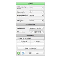
To implement the transceiver’s receiver mode, SLG46533 must convert a differential input to a single-ended output. This was done using an analog comparator. Figure 5 shows the ACMP3 configuration. The analog comparator is configured with 25-mV hysteresis and without low bandwidth in order to obtain higher-speed communications.
The selection of the ACMP is made based on the idea of using the same pins for differential input and differential output, as is required by a RS-485 transceiver. This is the main reason for choosing ACMP3, because it can have input pins with I/O control signals to configure them as an input or output for receiving or transmitting data.
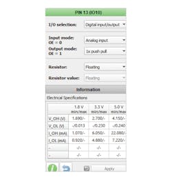
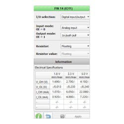
The inputs of the analog comparator are the differential inputs of the transceiver, called A and B. To do this, positive input of the ACMP is connected to Pin 13 (ACMP2 In+ source) and the negative input is connected to Pin 14 (the external VREF of the ACMP3).
When the transceiver flow-control bit is low, the transceiver works as a receiver of data. In this case, Pin 13 and Pin 14 are configured as analog inputs and the analog comparator processes both inputs to define a high or low level at its output. The output of the ACMP is connected to Pin 5, called R, which represents the received data. Figures 6 and 7 show the configurations of Pin 13 and Pin 14, respectively.
6. Pin 13 configuration.
7. Pin 14 configuration.
When the transceiver flow-control bit is high, the transceiver works as a data transmitter of data. In this case, Pin 13 and Pin 14 are configured as digital outputs. The single-ended serial data input to the transceiver is implemented with Pin 4, called D.
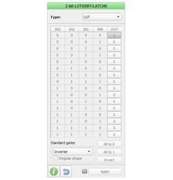
8. LUT0 configuration.
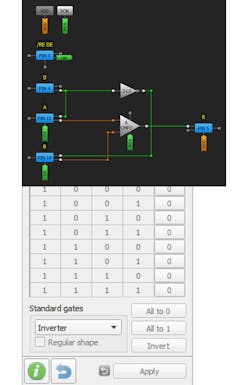
In order to obtain differential data at the outputs, LUT0 uses a NOT gate to obtain the inverse of the data input. Two signals (Data and its inverse) are connected to outputs A and B so that the differential data is transmitted to the bus. Figure 8 illustrates the LUT0 configuration.
The table above shows the logic states of inputs and outputs as well as the functionalities of the RS-422/RS-485 transceiver. The entire implementation is depicted in Figure 9.
9. RS-422/RS-485 block diagram.
Testing Results
To test the implementation, the transceiver was used as a receiver and a transmitter in separate cases. Therefore, the inputs and the outputs could be registered with a logic analyzer.
As a receiver, the RS-485 transceiver received a binary stream via the differential bus and the logic analyzer registered the differential inputs and the single-ended data output. The binary stream sent to the transceiver was:
1101001010
Figure 10 shows the received stream data at the inputs A and B, and the data output pin R. Furthermore, it can be seen that the flow-control signal /RE DE is set to a low logic level in order to configure the RS-485 transceiver as a data receiver.
10. RS-422/RS-485 transceiver in receiver mode.
As a transmitter, the RS-485 transceiver transmitted a binary stream (corresponding to the single-ended binary stream at the D input) via the differential bus. The logic analyzer registered the differential inputs and the single-ended data input. The binary stream sent by the transceiver was:
1001101010
Figure 11 shows the transmitted stream data by outputs A and B and the data input pin D. Also, the flow-control signal /RE DE was set to a high logic level in order to configure the RS-485 transceiver as a data transmitter.
11. RS-422/RS-485 transceiver in transmitter mode.
Conclusion
In this article, we implemented a RS-422/RS-485 transceiver with the SLG46533. RS-422/RS-485 transceivers are found in many applications that use this industrial bus because of its differential nature, which isn’t compatible with the single-ended nature of binary communication systems.
Several commercial ICs implement this type of transceiver. We created a compatible transceiver with the RS-485 specifications with respect to input differential voltage sensitivity, differential output voltage, typical data transfer rates, and typical common-mode voltages. Our system complies with RS-485 specifications, with the added benefit of much smaller IC size.
ADOM Ingenieria specializes in professional design, development, support and consulting in analog and digital electronic requirements.
