Photon/Phonon Conversion Sheds New Light on Optical Signal Processing
The processing of optical signals, with their real-time, streaming nature, would be greatly enhanced if there was a mechanism for writing, storing, and reading back the data. It’s the same situation with our familiar electronic data, of course, which is why “memory” is a major system function. Phonons—quanta of coherent acoustic vibrations—may offer a way to store and retrieve optical signals, and at a speed commensurate with the optical domain
To pursue this objective, researchers at the University of Sydney in Australia have demonstrated a buffer built as an optical waveguide that works by coherently translating the optical data to an acoustic hypersound wave. Optical information is extracted using a complementary process. The result is the storage of phase and amplitude of optical information with gigahertz bandwidth as well as multichannel operation at independent wavelengths, and with negligible crosstalk.
Their detailed paper in Nature, “A chip-integrated coherent photonic-phononic memory,” details the theory, actual implementation, and results. The objective is to develop components for storing or delaying optical signals, enabling mostly optical processing and thus the speed and performance benefits that development would bring. Signal “delay” is needed so that data can be briefly stored and managed inside the integrated device for processing prior to retrieval and transmission.
By using coherent phonons, the velocity of the optical pulse stream was reduced, leading to the ability to write and retrieve the optical data pulses as acoustic phonons. (Note that these hypersound phonons have wavelengths comparable to optical photons, but with velocity that’s five orders of magnitude lower.) Furthermore, optical data-transmission systems generally use multiple wavelengths to increase the overall capacity. Therefore, a storage process would be much more useful if it worked over a wide frequency range (supporting a large number of channels), and it must limit crosstalk between the optical channels.
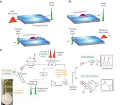
In the photonic-phononic memory, the storage process (a) uses an optical data pulse that’s depleted by a strong counter-propagating write pulse, storing the data pulse as an acoustic phonon. In the retrieval process (b), a read pulse depletes the acoustic wave, converting the data pulse back into the optical domain; all done using an experimental setup with a simplified basic schematic (c). The inset in the lower-left corner shows a chalcogenide chip containing more than 100 spiral waveguides of 6-, 11.7- and 23.7-cm lengths.
Their innovative approach (see figure) differs from existing schemes for coherent optical storage, as it uses acoustic phonons traveling in a planar, integrated optical waveguide. Since their buffer does not rely on structural resonance, it’s not limited to a narrow bandwidth or single wavelength operation.
The information carried by the optical signal is transferred to the acoustic phonons using stimulated Brillouin scattering (SBS)—a highly nonlinear optical effect—that results in coherent coupling between two optical waves and an acoustic wave. The intensity of the opto-acoustic interaction is increased several orders of magnitude by using carefully designed waveguides that guide optical as well as acoustic waves, allowing storage of broadband optical signals in a planar waveguide without relying on a resonator geometry. (Note that this is a greatly simplified representation, as the actual setup includes a continuous wave, single-sideband, or SSB, modulator; intensity modulator; pulse generator, bandpass filter, photodetector, local oscillator, and Brillouin frequency shifter; additional details are here).
A strong optical-write pulse, offset by the acoustic-resonance frequency of the optical-waveguide material, propagates counter to the optical data pulse. When the two pulses meet, the resultant beat pattern between them compresses the material periodically (a process called electrostriction), and excites resonantly and locally a coherent acoustic phonon.
For the storage medium, they used a spiral waveguide made from the chalcogenide glass (materials containing one or more of the chalcogen elements such as sulfur, selenium, and tellurium, and the most suitable for SBS) with a “rib” waveguide structure having a cross-section of 2.2 μm by 800 nm, with more than 100 spirals that have lengths ranging from around 9 to 24 cm. The overall chip length is about 30 mm.
The team used six different amplitude levels in the first pulse, and maintained the amplitude level of a second data pulse constant as a reference. A comparison of the original and retrieved pulse demonstrated that they were able to easily distinguish among the six different amplitude levels. Thus, they were able to confirm the multi-wavelength capabilities of their memory, with operation at several different wavelengths along with minimal crosstalk between those multiple-wavelength channels.


