Download this article in PDF format.
Whether you’re designing integrated circuits, equipment, or systems, you absolutely must provide protection from electrostatic discharge (ESD). ESD is a common problem in most environments. Product failures from ESD lead to enormous reliability issues that can increase costs, drive customers away, and give your products a poor reputation.
Designing in ESD protection may be a boring process, but it’s an essential part of creating new circuits or equipment today. It’s one of those things that you don’t have to like, but need to do if you’re going to avoid having your products labeled as a catastrophe. The good news is that multiple solutions are available to make adding ESD protection fast and easy.
Sponsored Resources:
- Critical selection parameters and standards ratings for ESD protection devices
- System-level ESD protection
- ESD224 HDMI 2.0 Compliance and Protection
Explaining ESD
ESD is that sudden transfer of static electric charges from one object to another, where each object has a different electrostatic potential. Almost all objects will pick up a charge of electrons when it touches some other object. Walking on a carpet will cause you to pick up a charge of many volts that will be felt as a momentary shock when touching some nearby metal object. Handling anything plastic, such as a Styrofoam cup or plastic bag, will cause a charge build up.
This difference of charges represents hundreds or even thousands of volts. When the two objects with different charges are brought together and touch, the resulting transfer of electrons produces a high current flow. The results are thermal levels that can melt material or the breakdown of dielectrics in an IC. The outcome is usually a catastrophic failure of semiconductor devices.
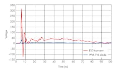
1. Shown is a typical ESD transient pulse and how it can be suppressed with a TVS diode.
Figure 1 shows what a common ESD pulse looks like (red curve). The transient duration is short, typically several nanoseconds, but mostly less than 100 ns. Such destructive pulses can be minimized by connecting a transient-voltage-suppressor (TVS) diode from the signal line to ground. The TVS diode is like a Zener that conducts and clamps the voltage at some safe lower level. The result is the blue curve.
The most vulnerable devices are ICs made of MOSFETs or discrete MOSFETs. These transistors have a tiny gate with a super-thin dielectric that’s easily broken down with ESD. Today, most CMOS ICs and discrete MOSFETs incorporate some minimal internal ESD protection. While the internal protection eliminates some problems, it may be inadequate in other applications. Therefore, many products also incorporate external ESD protection.
As MOSFET sizes decreased over the past years to increase switching speed and reduce chip space, these devices have become even more susceptible to ESD. Internal chip protection routinely needs external assistance to curb the eventual exposure to ESD during product assembly, testing, shipping, or usage.
Any product with a high-speed interface, such as HDMI, Ethernet, or USB, is especially susceptible to ESD if it has an external connector to the outside world where humans can come into contact. Audio and RF antenna connections are also vulnerable. It only takes one ESD strike to permanently damage a product, which makes ESD protection a critical part of a system design.
The most common way to protect sensitive inputs and outputs of an IC or other circuit is to connect a TVS diode between the line carrying the signal and ground. If an ESD pulse occurs, the diode will shunt the resulting current to ground protecting the circuitry. External protection diodes are available to ensure that no damage occurs. To specify an ESD TVS diode, you need to understand the critical selection parameters and standards ratings for ESD protection devices.
ESD Diode Selection
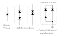
ESD protection diodes are similar to Zener diodes in that they’re designed to conduct at a certain voltage level. Common schematic symbols for these TVS diodes are shown in Figure 2. The back-to-back connected Zeners protect against both positive and negative transients.
2. Common ESD protection diode schematic symbols include Zener diode TVS (a), bidirectional TVS (b), and functional configuration of a bidirectional TVS (c).
What follows are the most common ESD specification parameters:
- Working voltage: This is the main voltage rating that states the level where the devices begins to clamp and limit the voltage. It must be higher than the logic-signal voltage levels to avoid compromising the signal integrity. The voltage level may be positive, negative, or both.
- IEC rating: The International Electrotechnical Commission (IEC) has the standard 61000-4-2, which states the amount of voltage that the device can withstand. Two measures are given—the contact voltage and the air-gap voltage. Contact voltage is the transient discharged directly into the protected device. The air gap voltage is the transient level discharged into the device via an air gap. Four levels are given, with the highest level 4 specifying 8-kV contact voltage and 15-kV air-gap voltage.
- Capacitance: When a protection diode is connected from the signal line to ground, it adds shunt capacitance that will extend signal rise and fall times and seriously limit the data rate. This capacitance must be small (< 1 pF) to maintain good signal integrity. Eye-diagram tests are routinely used to see if the signals meet the requirements of the standards.
- Clamping voltage: This is the voltage level where the diode conduction kicks in and limits the level to the IC. The clamping voltage is generally extrapolated from a transmission-line-pulse (TLP) curve that shows the relationship between the clamping voltage and diode current. The TLP curve is usually given in the datasheet.
- Channels: Interfaces have multiple signal lines that are present at connectors. Each line is a channel and all of them need to be protected. Multichannel ESD protection devices are available to simplify and minimize PCB layout.
To select an ESD component, consider Texas Instruments’ line of ESD protection devices that can handle almost all common applications.
ESD Design Process
Based on the design factors given earlier, here is a step-by-step procedure for selecting an ESD diode.
1. Determine the number of channels (IC pins or interface lines) to be protected.
2. Determine the logic voltage range of each channel on the device or interface. Most are positive voltages of 5 V or less. The protection diode’s working voltage should be a little bit higher than the maximum expected logic voltage.
3. Determine if you need a unidirectional or bidirectional protection diode. A unidirectional diode is typically all that’s required unless bipolar logic voltages are involved.
4. Determine the maximum possible capacitance that the device or interface line can withstand. It helps if an overall capacitance budget is known. Otherwise keep the capacitance of the diode as low as possible.
5. Determine the clamping voltage. It should be as low as possible, but not interfere with normal operations. Estimate the clamp level from the TLP curve in the datasheet.
6. A good rule of thumb is to also specify a diode that meets the IEC 61000-4-2 level 4 specifications of 8-kV contact voltage and 15-kV air-gap voltage.
Texas Instruments offers several selection and design tools to help you choose products appropriate and most of the popular interfaces.
Design Example
Consider the goal to protect an HDMI 2.0 interface. The High Definition Multimedia Interface is widely used in consumer video and audio connectivity. The cables and connectors are routinely handled by humans and subject to considerable instances of ESD. ESD diodes eliminate the problem.
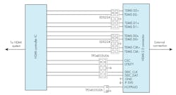
3. In this example of using a four-channel ESD device on an HDMI 2.0 interface, the data lines are protected with two ESD224 devices while the auxiliary lines are protected with TPDxE05U06 devices.
Figure 3 shows the typical basic HDMI data connections. The HDMI interface consists of four differential pair data lines (3 data, 1 clock) and six other control and data lines. All should be protected. Typical logic levels are 3.3 V. One approach is to use the TI TPD1E05U06 single TVS device; one for each data line. Alternatively, you can use the TPD4E05U06 that contains four TVS devices. Two of these ICs handle the four differential data lines.
Another choice is TI’s ESD224, a bidirectional TVS ESD protection diode array for high-speed applications. The ESD224 employs four on-chip, differentially matched series elements to enhance downstream ESD clamping performance while maintaining the signal compliance for HDMI. The goal of the ESD224 is to provide a low clamping voltage device while still being able to pass HDMI 2.0’s 6-Gb/s signals. For more detail on the ESD224, see the information at the link below.
More information on ESD and its mitigation is available in Texas Instruments’ series of short (<4 minute), easy-to-digest videos that explain all of essentials required to protect against ESD.Sponsored Resources:
- Critical selection parameters and standards ratings for ESD protection devices
- System-level ESD protection
- ESD224 HDMI 2.0 Compliance and Protection
References
Vinson, J., Bernier, J., Croft, G., and Liou, J., ESD Design and Analysis Handbook, Kluwer Academic Publishers, 2003.
Wang, A., On-Chip ESD Protection of Integrated Circuits, Kluwer Academic Publishers, 2002.


