The goal of embedding our ubiquitous, silicon-based ICs with high-speed optical interconnects without need for intervening electro-optical conversion (and its complement) may be a step closer to reality. A team at MIT, headed by associate professor of physics Pablo Jarillo-Herrero, has devised a way to use a sophisticated material to bridge the gap, overcoming the impediments that naturally exist among silicon, light emission/capture, and optical wavelength
In their paper “A MoTe2-based light-emitting diode and photodetector for silicon photonic integrated circuits” published in Nature Nanotechnology, along with extensive supplementary information, researchers at Massachusetts Institute of Technology detailed their demonstration efforts. The underlying materials problem is that silicon, despite its many wondrous electrical and mechanical properties, isn’t compatible with optical requirements. Most semiconductor materials emit light in the visible range, and silicon absorbs light at these wavelengths.
They developed a silicon waveguide-integrated light source and photodetector based on a P-N junction of bilayer molybdenum ditelluride (MoTe2), which is an ultrathin semiconductor in a group of materials known as two-dimensional transition-metal dichalcogenides (TMDs). MoTe2 emits light in the infrared range, and thus isn’t absorbed by silicon. Therefore, it can be used for on-chip communication.
1. Sketch of a device based on encapsulated monolayer MoTe2, with separation of the split metal gates is 200 nm; the flake width is about 5 μm (a). Optical image of the monolayer device before the source-drain metal electrodes evaporation (b). (Source: MIT and Macmillan Publishers Limited/Springer Nature)
To use the material as a light emitter, the researchers first had to convert it into a P-N junction diode, which is done by introducing chemical impurities into the substrate material. In contrast, the 2D molybdenum ditelluride can be mechanically attached to any material; then a voltage is applied across metallic gate electrodes placed side-by-side on top of the material (Fig. 1). Prof. Jarillo-Herrero notes, “So by using diodes made of molybdenum ditelluride, we are able to fabricate light-emitting diodes (LEDs) compatible with silicon chips.”
The device can also be configured to function as a photodetector by reversing the polarity of the voltage applied to the device. This causes it to stop conducting electricity until light shines on it, at which time the current flow resumes. In this way, the devices are able to both transmit and receive optical signals.
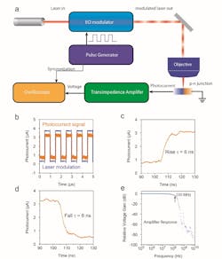
The research team believes that these emerging two-dimensional TMDs could provide an approach to developing optical interconnect components that could integrate with silicon photonics and CMOS processing (Fig. 2). Most telecommunication systems operate at optical wavelengths of 1.3 or 1.5 μm, while molybdenum ditelluride emits light at 1.1 μm. This makes it compatible with silicon ICs, but not a fit for telecommunications systems. For this reason, 1.3-/1.5-μm emission and detection wavelengths would simplify fabrication of optical-fiber links.
2. The experimental setup used for measuring the time response of the p-n junction (a); photoresponse of bilayer MoTe2 p-n junction used to modulated the laser at 1 MHz (b); details of the rising (c) and falling edges (d); frequency response of the test setup’s transimpedance amplifier, with 3-dB rolloff near 150 MHz (e). (Source: MIT and Macmillan Publishers Limited/Springer Nature)
To achieve this, the researchers are investigating black phosphorus, an ultrathin material that can be “tuned” to emit light at different wavelengths by changing the number of layers of material used. By doing so, they hope to develop devices with the number of layers needed to emit light at those two wavelengths yet retain the compatibility with silicon.
Jarillo-Herrero acknowledged that the results of the research, which was supported by the Center for Excitonics (an Energy Frontier Research Center funded by the U.S. Department of Energy), are a proof of concept and far from commercialization. Nonetheless, “the hope is that if we are able to communicate on-chip via optical signals instead of electronic signals, we will be able to do so more quickly, and while consuming less power,” he added.


