Regulator Review: Wring the Best Performance Out of Your LDO
Download this article in PDF format.
A low-dropout (LDO) regulator is a simple, inexpensive way to generate a regulated output voltage from a higher-voltage input. It’s inherently low-noise because it has no switching transients, and it requires few if any external components, so it takes up little board space.
The LDO is easy to use right out of the box, but that doesn’t mean its performance can’t be improved. In this article, we’ll review the principles of operation of the standard regulator and the LDO, and discuss a couple of ways to boost its noise performance.
Sponsored Resources:
Transforming a Standard Regulator into an LDO
A linear regulator is inefficient because it dissipates power across the regulation device to regulate the output voltage. The regulation device is typically a power transistor—either a bipolar device or a FET.
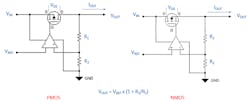
1. The basic PMOS and NMOS linear regulator architectures. (Source: TI Training: LDO Basics—Dropout Voltage video)
Figure 1 shows MOSFET linear-regulator circuits with both PMOS and NMOS power transistors. In both circuits, the voltage across the regulator’s power transistor is:
VDS = VIN - VOUT = IOUT × RDS
where RDS is the FET’s drain-to-source resistance. VDS depends on the FET’s gate-to-source voltage (VGS).
The regulator control circuit uses R1 and R2 to divide down VOUT and compares the scaled value to a reference voltage (VREF). The resulting error signal drives the FET’s gate voltage (VG); this, in turn, controls VGS to regulate VOUT against changes in load current (IOUT) or input voltage (VIN). In these basic designs, VG can range between the error amplifier’s positive and negative supply rails: VIN and ground.
The minimum allowed value of VDS is called the dropout voltage (VDO). For proper operation, VIN ≥ VOUT + VDO. If VIN falls below this value, the regulator will drop out of regulation and will not be able to maintain the desired output. Instead, the output voltage will track the input voltage minus the dropout voltage.
As its name implies, an LDO is designed to minimize the value of VDO. A state-of-the-art LDO can produce a regulated output with a dropout voltage as low as 100 mV. With the spread of low-voltage, power-efficient designs, LDOs are the dominant linear regulators today.
How do we turn a standard regulator design into an LDO? At the design stage, a larger-size power FET will yield a lower dropout voltage because it has a lower resistance. However, the architecture of the circuit is the main determining factor, especially the minimum and maximum values of VGS.
The P-channel MOSFET (PMOS) design requires a negative VGS to operate. If either VIN or IOUT increases, the control circuit responds by driving VGS more negative. In the PMOS case, VS = VIN. The maximum negative VGS occurs when driving VG to the negative rail; this corresponds to VGS = – VIN. Reducing the dropout voltage (VIN – VOUT) doesn’t affect the magnitude of VGS, making an LDO design possible.
For the N-channel MOSFET (NFET), the situation is reversed. If VIN decreases, the control circuit must drive VG more positive to increase VGS. The error amplifier can still drive VG between VIN and ground, but now VS = VOUT, so the maximum value of VGS is (VIN – VOUT)—in other words, the voltage across the FET.
A FET doesn’t even begin to turn on until VGS is greater than a threshold voltage of about 2 V. The NMOS circuit as shown limits the minimum dropout voltage to 2 V, not exactly LDO territory.
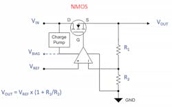
2. Here, the basic NMOS circuit is modified to enable LDO operation. Either a charge pump or an external bias voltage can be used. (Source: TI Training: LDO Basics—Dropout Voltage with Jose Gonzalez video)
Adding an internal charge pump between VIN and the error amp’s positive supply solves the problem (Fig. 2). The charge pump boosts the error amplifier’s positive rail, allowing it to drive a higher VGS, and making an LDO design possible. An alternative implementation supplies the higher positive rail via an external BIAS pin. Ultra-low-dropout LDOs such as TI’s new TPS7A10 use this approach.
As we’ve discussed, low noise is an advantage of a linear regulator or LDO, and many applications use an LDO to clean up the noisy output of a switching power converter. Two parameters in the datasheet characterize the LDO’s noise performance, so we’ll discuss these now.
Input Noise and PSRR
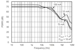
The power-supply rejection ratio (PSRR), also called the power-supply ripple rejection, describes how well the LDO rejects noise from an external source, such as a switching power supply, that appears on its input. The PSRR compares the output ripple and the input ripple of the LDO over the frequency range of interest for the application. Figure 3 shows the graph of PSRR vs. current for the TPS717, a low-noise, high-bandwidth PSRR LDO with 150-mA maximum output.
3. The TPS717 features a high-bandwidth, high-gain error loop gain for high PSRR. (Source: TI “TPS717” PDF)
PSRR is expressed in decibels (dB)—the higher the number, the better the rejection. The equation is:
A couple of factors can affect the PSRR. An increased load current affects both ends of the frequency range. The output impedance of the FET is inversely proportional to the drain current, so an increase in IOUT lowers the PSRR at lower frequencies because it lowers the error-loop gain. At the same time, increasing the load current moves the output pole to higher frequencies. This increases the feedback loop bandwidth, which increases the PSRR at higher frequencies.
The PSRR also lowers when VDS drops below about 1 V because the FET begins to transition from the active (saturation) region of operation into the triode/ohmic region, which also causes the feedback loop to lose gain.
When comparing PSRR performance between LDOs, it’s important always to match VIN-VOUT and load currents. It’s also important to compare LDOs with identical VOUT, since PSRR is usually better at lower output voltages.
Output Noise and Spectral Noise Density
Of course, the LDO itself isn’t noiseless. It generates internal (intrinsic) noise that appears on the output and adds to the residual input noise discussed above. Several physical mechanisms contribute to intrinsic noise in LDOs and other components.
Thermal noise occurs in both active and passive devices due to the random motion of charge carriers (either electrons or holes) in a conductor. Thermal noise is proportional to absolute temperature and is independent of current flow. It has the flat spectrum characteristic of white noise.
Flicker noise occurs only in active devices and varies by technology. Flicker noise is proportional to current flow and inversely dependent on frequency, hence its other name of 1/f noise.
Finally, shot noise is caused by electrons or holes randomly crossing a potential barrier such as a PN junction. It’s also associated with current flow and has a flat frequency spectrum.
Intrinsic noise is expressed in µV√Hz; it’s characterized by an output spectral noise density graph in the LDO datasheet showing how the noise varies over frequency. Datasheets typically include several graphs that describe how the output noise varies with output current (IOUT), output voltage (VOUT), and other parameters.
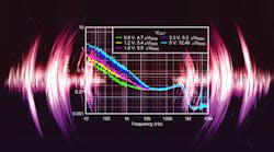
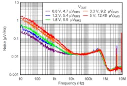
Figure 4 shows the spectral noise density versus VOUT for the TPS7A91, a 1-A high-accuracy low-noise LDO with 200-mV maximum dropout voltage.
4. The spectral noise density of an LDO increases with VOUT at lower frequencies. (Source: TI Blog: “LDO basics: noise—part 1”)
The output noise is concentrated at the lower end of the frequency spectrum. Datasheets commonly provide a single noise value for comparison purposes. This value represents the output noise integrated from 10 Hz to 100 kHz and is expressed in microvolts root-mean-square (μVRMS). Using this metric, the TPS7A91’s output noise figure is 4.7 μVRMS.
Be careful when comparing components from different manufacturers. Some datasheets integrate the noise over another frequency range, such as 100 Hz – 100 kHz, or even use a custom range. Integrating over a select frequency range can help mask unflattering noise properties, so it’s important to examine the individual noise curves in addition to the integrated value.
To Improve LDO Noise Performance, Start with the Voltage Reference
How do we improve the noise performance of the standard LDO? Although every component in the LDO contributes to the overall noise, the voltage-reference circuit is the main culprit. There are two reasons: the circuit has many noise-generating active and passive components; and any noise on VREF is amplified by the error amplifier. Any input ripple that appears on the reference is also amplified and appears on the output; therefore, the bandgap reference must have high PSRR as well as low noise.
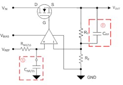
The solution for both internal noise and PSRR is simply to add a low-pass filter (LPF) in series with the bandgap reference output. As shown in Figure 5, this LPF is accomplished by adding an external capacitor CNR/SS to the existing internal resistor RNR/SS, and many low-noise LDOs include a pin for this purpose.
5. Adding a noise-reduction capacitor (1) and a feed-forward capacitor (2) can improve LDO noise performance. (Source: TI Blog: “LDO basics: noise—part 2,” Fig. 1)
The capacitor serves a dual purpose: when the LDO is initially powered up, the VREF voltage seen by the error-amplifier ramps up as CNR/SS charges through the internal resistor. In effect, the LPF adds a soft-start, hence the “NR/SS” subscript on the resistor and capacitor. This soft-start is helpful in preventing a current-limit condition if the LDO must charge a large-value output capacitance at startup.
The LPF isn’t a panacea. Adding it reduces the PSRR at low frequencies because it passes bandgap ripple in this range. A low-ESR ceramic output capacitor improves PSRR performance. The capacitance value should be chosen based on the frequencies that are important for the application. Careful board layout design will reduce the ripple feedthrough from input to output caused by board parasitics.
Another strategy to prevent the output noise from being amplified by the error amplifier is to add a feed-forward capacitor. CFF provides an ac bypass around resistor R1, leaving the dc gain unchanged but reducing the gain at higher frequencies.
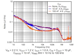
Adding a feed-forward capacitor has multiple effects on LDO performance, including improved noise, stability, load response, and PSRR. It also improves the phase margin of the feedback loop, enhancing the LDO’s load transient response with less ringing and faster settling time.
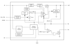
6. The TPS7A91 is an adjustable-output LDO optimized for low-noise operation. (Source: TI “TPS7A91” PDF)
7. Adding a feed-forward capacitor CFF improves the TPS7A91’s output noise performance at lower frequencies. (Source: TI Blog: “LDO basics: noise—part 2,” Fig. 2)
A feed-forward capacitor can’t be added to a standard three-terminal fixed-output LDO because the R1/R2 node is internal. Still, many LDOs designed for low-noise operation make this node available on a pin. Of course, adjustable-output LDOs such as the TPS7A91 in Figures 6 and 7 include a pin (FB) for external resistors and CFF. This device also features a CNR/SS pin.
The table provides a summary of the effects versus frequency of the two noise-reduction techniques discussed above: CNR and CFF.
Conclusion
The LDO is the dominant architecture for linear regulation. This article discussed the two main FET LDO architectures, the sources of noise, and reviewed techniques to help improve noise performance. For a deeper discussion of LDO noise, go here. PSRR is discussed in more detail here, and you can find out more about using an LDO feedforward capacitor in this application report.
Texas Instruments offers over 500 LDOs for different applications, giving the designer a broad range of features: low noise, wide VIN, small size, low Iq, and processor attach.
Sponsored Resources:
