Two of the most often used amplifier building blocks in audio amplifier design are the common emitter amplifier with emitter degeneration and the emitter follower using the same circuit biasing. The emitter amplifier is the simplest and most often used tool to create voltage gain. The emitter follower is generally used as a voltage buffer and helps drive loads.
Here, both will be demonstrated through simulation using LTSpice and a simple breadboard prototype. Specifically, the examples will be prototyped with the 2N5401 PNP transistor (if necessary) and 2N5551 NPN transistor. In addition, for the input stimulus to the circuits, a 1-kHz waveform will be used which will be generated from YouTube and applied to the circuit through an AUX cable breakout circuit.
Quick Note on Power Supply Used in Tests
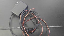
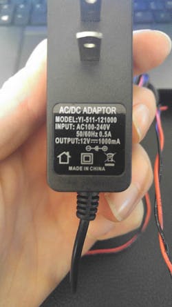
For these quick breadboard prototypes, a 12-V wall-wart power supply was chosen (Figs. 1 and 2). In general, wall-wart power supplies are readily available and cheap. Most people reading this probably have many of them laying around that may not be of use to them anymore. This makes them perfect as a source of power for breadboard prototypes.
1. Wall-wart power supply.
2. The supply was made in China!
However, one must understand that these power supplies are usually pretty noisy. By that I mean the output voltage is generated through a switch-mode power supply running at some specific frequency. This creates ripples on the voltage at the same frequency, which can be a source of distortion in circuits and probably cause problems if not given any thought.
Luckily, this noise can easily be filtered out. Passive RC filters, active filters, and many times LDOs are used to eliminate this noise reliably. Another oft-used simple method to help with the noise involves adding decoupling capacitors to the power supply. A quick glance at many circuits today and you can see that almost all ICs on printed circuit boards (PCBs) have small decoupling caps on each power-supply pin.
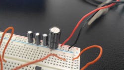
3 Decoupling caps are added to breadboard.
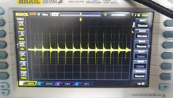
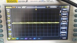
Figure 3 shows how adding decoupling caps to the breadboard can improve the integrity of the power-supply voltage. The oscilloscope screenshot in Figure 4 shows the supply connected directly to the oscilloscope probes (ac-coupled). In Figure 5, the same power-supply voltage with a single 1-µF capacitor is connected from VCC to GND. Notice that the noise on the power-supply line is greatly reduced when adding only a single capacitor.
4. Ripple on power-supply rail.
5. Power-supply rail with a 1-µF cap connected from VCC to GND.
Amplifier Circuit
The common emitter amplifier and emitter follower will be demonstrated using the same amplifier circuit. The main difference between the two will be where the output is taken. For the common emitter amplifier, we will take the output at the collector of the transistor. For the emitter follower, the output will be taken at the emitter of the transistor.
The emitter-follower amplifier, often used in amplifier output stages, is known as a class A amplifier. The class A amplifier consists of a transistor that’s always ON. Current is always flowing through the collector, and an output is produced for the entire 360-degree cycle of the input. It’s used to drive the load, which is commonly a speaker with an impedance of 2, 4, or 8 Ω.
To begin, we’ll simulate the circuit to be tested in LTSpice. LTSpice is a great tool for hobbyists, professionals, and any person interested in studying and understanding circuits. It’s free, easy to learn and use, and many resources are readily available on the web.
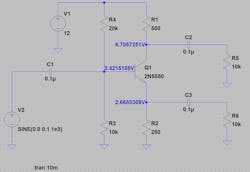
6. LTSpice schematic of the circuit to be tested.
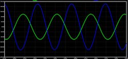
Figure 6 illustrates the circuit that will be tested on the breadboard. We won’t go over the details of biasing the transistor, but want to note that the transistor was biased with the intent of having approximately 10 mA of current. Plots of the voltage output taken at the collector (Fig. 7) and the emitter (Fig. 8).
7. LTSpice plot of the output taken at the collector of transistor.
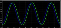
8. LTSpice plot of the output taken at the emitter of the transistor.
The plots reveal fundamental properties of the two amplifier types. First, as Fig. 7 shows, the amplifier has a gain of approximately 2 when the output is taken from the collector. Also, the output is close to 180 degrees out of phase from the input. If the small signal gain of the circuit is derived, this will also be shown by the mathematical transfer function. The gain depends on the collector and emitter resistors; a good approximation is collector resistance divided by emitter resistance.
On the other hand, when the output is taken at the emitter (Fig. 8, again), the signals are close to in-phase with one another and the gain is approximately unity. Once again, this also matches what would be shown by the small signal transfer function.
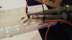
9. Class A amplifier breadboard prototype.
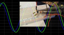
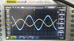
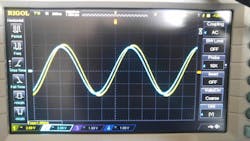
Next, the breadboard circuit is built and tested (Fig. 9). Figs. 10 and 11 show the plots taken on the oscilloscope for the corresponding outputs at the collector and the emitter, respectively.
10. Plot showing the input and output signals taken at the collector.
11. Plot showing the input and output signals taken at the emitter.
Looking at the plots, we can see that the waveforms closely match the expected simulated waveforms. It’s good practice to first design your circuits on paper if possible, then simulate the circuits, and finally prototype and test your circuits and see how close they match your expected results.
We can see from the plots in Figs. 10 and 11 that the simulations closely match the measured results in both amplitude and phase. For simplicity, the paper calculations have been left out of the documentation. However that doesn’t mean they’re not important. If your circuit doesn’t work on paper, it will not work in simulation or on the breadboard. Paper calculations should always be the starting point and, in my opinion, are the most important part of the design.
Wrap Up
We have presented two different types of building blocks commonly used in audio amplifier design. The amplifiers serve two different purposes, with one being a voltage gain block and the other being a unity gain voltage buffer. These were both derived, simulated, and prototyped with closely matching results. In addition to audio, these circuit blocks find use in all types of applications. A good understanding of the amplifiers’ operation and properties will help all circuit designers from many different disciplines.
