Graphene and Gold Merge to Deliver Superior Photodetector
Graphene seems to be following a trajectory somewhat paralleling that of the first laser. When the latter was publicly announced in 1960, pundits and skeptics remarked that it was “a solution looking for problems to solve.” Of course, we know how that assessment turned out, as the laser is not only an indispensable tool in the design kit, but it also has been the enabling component in countless applications not even envisioned at the time (you can make your own lengthy list, of course).
Similarly, when graphene—a sheet of a single layer of carbon atoms, tightly bound in a hexagonal honeycomb lattice—was developed in the early 2000s (and for which physicists Sir Konstantin Sergeevich Novoselov and Sir Andre Konstantin Geim, both at the University of Manchester UK received the Nobel Prize in 2010), there wasn’t the same “snarkiness.” Still, there were legitimate questions as to what its “real world” applicability might be. The reality is that it’s finding many innovative uses in batteries, super-light and super-strong materials, and more.
It’s even finding its way into photodetectors, a vital energy-transducing component in many electro-optical systems. A research team supported by the Department of Energy at the UCLA Samueli School of Engineering has now used it, along with gold and semiconductor processing techniques, to create a greatly improved photodetector. Although related to photovoltaic cells, which are used to generate useful power from impinging light, these photodetectors are primarily involved with imaging or measuring light intensity, such as in thermal imaging for night-vision goggles and many medical applications.
There’s always a tradeoff among primary photodetector parameters of operating speed, sensitivity and internal noise, and bandwidth. The tradeoff is a function of materials used, design arrangement, doping, and fabrication techniques. In general, when trying to enhance one of these three factors, there’s usually a detrimental impact on the others. For example, increasing bandwidth usually reduces all-important sensitivity. For this reason and others, photodetectors are usually carefully tailored to the intended application to provide the optimum balance among specifications.
Graphene Ups and Downs
Research results are detailed in their paper “Gold-patched graphene nano-stripes for high-responsivity and ultrafast photodetection from the visible to infrared regime” and supplemental information published in Light: Science and Applications. The researchers explain that graphene is a potentially good material candidate due to multiple factors: its unique band structure, which enables carrier generation via optical absorption over an extremely broad spectral range from the ultraviolet to microwave regime; its high electron/hole mobility and weak scattering, which enables an ultrafast response; its two-dimensional nature allows multiple electron/hole pairs to be generated for a single absorbed photon; and photodetectors based on graphene are compatible with silicon-based fabrication.
However, developing an effective graphene-based photodetector faces several obstacles. Most graphene photodetectors use graphene-metal junctions or graphene p-n junctions to separate and extract photogenerated carriers. The low optical absorption inside graphene-metal or graphene p-n junction regions (~100-200 nm) used to separate and extract photogenerated carriers, plus the short photocarrier lifetime of graphene (~1 ps), are barriers to developing high-responsivity graphene photodetectors.
A Different Tack
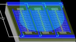
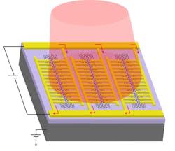
1. Schematic of the photodetector developed by UCLA engineers, showing gold comb-shaped nanopatterns on top of graphene nano-stripes (hexagonal structures) and light source (pink cylinder). (Image source: UCLA)
In this new approach, the team combined standard techniques used to build photoconductive nanostructures based on gold-patches interleaved with graphene nano-stripes (Fig. 1). This structure has electrical and optical characteristics that enable simultaneous broadband and ultrafast photodetection with high responsivity.
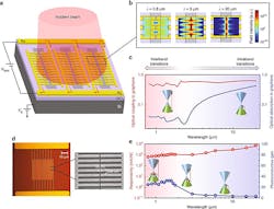
The gold comb-like nanoscale patterns are about 100 nm wide, with the graphene functioning as a grid-like net, grabbing photons and converting them into electrical signals. The nanopatterns transfer the electrical signals to a processor that creates a high-quality image even under low-light conditions. The final device has an active area of 30 × 30 μm2 (Fig. 2).
2. Schematic of a photodetector based on gold-patched graphene nano-stripes with gold patches having a width of 100 nm, periodicity of 200 nm, height of 50 nm, length of 1 μm, and a tip-to-tip gap size of 50 nm (a). Plot of the transmitted optical field through the gold patches at 0.8, 5, and 20 μm, indicating highly efficient and broadband optical coupling to the graphene nano-stripes (b). Estimates for the optical coupling (red curve) and optical absorption (blue curve) in the graphene nano-stripes as a function of wavelength (c). Optical and scanning electron microscope images for a fabricated photodetector based on gold-patched graphene nano-stripes (d). The measured responsivity (red data) and photoconductive gain (blue data) of the fabricated photodetector at an optical power of 2.5 μW, gate voltage of 22 V, and bias voltage of 20 mV (e). (Source: UCLA)
The team assessed sensitivity and bandwidth as well as other performance factors across multiple values of bias and gate voltage, temperature, and other variables. They reported that the photodetector has ultrabroad operation from the visible to the infrared regime, with responsivity ranging from 0.6 A/W (at 0.8 μm wavelength) to 11.5 A/W (20 μm wavelength). For bandwidth, they used a pair of tunable distributed-feedback (DFB) lasers in a complex test arrangement and found no roll-off up to 50 GHz—the limit of their setup (Fig. 3). Experimental results were in close agreement with their modeled versions.
3. To characterize the operation speed of the fabricated photodetector, beams from two DFB lasers at frequencies of f1 and f2 are focused onto the gold-patched graphene nano-stripes to generate a photocurrent, Iph, at the optical beating frequency, f1-f2. The measured photoresponse values exhibit no roll-off up to 50 GHz, which is the frequency limitation of the utilized experimental setup. The dashed lines show the estimated frequency response for the graphene photodetector calculated from the device electrical model. (Source: UCLA)
“We specifically designed the dimensions of the graphene nano-stripes and their metal patches such that incoming visible and infrared light is tightly confined inside them,” says Semih Cakmakyapan, a UCLA postdoctoral scholar and the lead author of the study. “This design efficiently produces an electrical signal that follows ultra-fast and subtle variations in the light’s intensity over the entire spectral range, from visible to infrared.”


