When it comes to designing electronic products, custom silicon really is the gold standard. Having custom SoCs designed specifically for your application delivers an optimized solution in terms of power efficiency, performance, board space, and bill-of-materials (BOM) costs. Taking the custom approach also enables solutions with unique capabilities that would be difficult to achieve using off-the-shelf hardware, and it creates devices that are difficult to reverse-engineer, giving IP security.
However, ASICs are notoriously expensive to create and time-consuming to design—or are they?
In fact, recent changes in the semiconductor industry mean many of the preconceptions about custom chip design are no longer true. So, let’s bust these myths!
1. ASICs are expensive to manufacture.
High-volume consumer electronics markets create demand for advanced process nodes. As a result, the capacity within foundries using larger process nodes has increased. Mature nodes may not be suitable for bleeding-edge, highly integrated, and high-performance digital ICs, but they remain ideal for mixed-signal solutions.
To maximize foundry utilization and return on investment, manufacturers have taken steps to attract customers, such as significantly lowering their engineering costs. Manufacturers can afford to make these cost reductions because the bulk of the cost of the fab has already been recovered. Furthermore, the increase in availability of capacity based on mature process nodes is keeping those costs low, which means it’s more affordable than ever to create custom silicon.
2. Very high volumes are needed to make custom chips worth it.
Good design houses with strong engineering talent and deep IP libraries can generate huge BOM savings. This is particularly relevant for designs that feature significant analog/mixed-signal functionality or are currently based on FPGA technology. Switching to a custom ASIC can remove redundancy and consolidate functionality, generating significant BOM savings that can easily reach well over 50%.
The average selling price of discrete solutions is subject to market influences, manufacturer’s strategies, and, as many device manufacturers are now fabless, the overall merchant foundry landscape. These factors are largely eliminated when the majority of functionality is consolidated into a single device, which means ASICs can make good engineering and business sense even at medium or low volumes.
3. Custom silicon is expensive to design.
The availability of IP changed the way integrated circuits are designed, from handcrafting every function at the transistor level to using building blocks that have been verified to work together. Over a relatively short number of years the cost of designing custom silicon has fallen drastically, meaning it’s probably comparable to other design costs. Experienced design houses have significant existing silicon-proven IP libraries they can leverage, which keeps costs low. With a focus on engineering with minimal overheads, design houses can deliver a turnkey experience that’s often more affordable than you would expect.
4. Creating custom silicon designs is time-consuming.
A custom design doesn’t mean having to design everything from scratch; good design houses now leverage existing silicon-proven IP libraries, which greatly reduces design time. In addition, they will have well-designed process flows to speed time-to-market. S3 Semi has a large portfolio of silicon-proven IP; we know it works, so fast design also comes with the assurance that the design is going to work the first time.
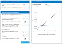
One can use S3 Semiconductors’ online calculator to see if shrinking a board onto a custom integrated circuit is an economical option for a given application.
Being able to leverage the time-to-market benefits of designing at a higher level of abstraction is something the entire industry strives for, but it’s really only available when working with custom silicon. By starting with a predefined platform, based on IP that has been verified in your targeted process node to fulfill the function you need, is founded on IP reuse. So, custom design isn’t synonymous with starting with a blank page every time.
5. Analog/mixed-signal is hard.
There are many aspects involved in being a digital- or analog-domain expert, but mixed-signal integration involves working in both domains and dealing with the issues that will inevitably arise through this added level of complexity. Engineers will need to understand the effect that high-frequency digital can have on sensitive analog, for example, or how linear amplifiers may impact digital slew rates. Working with a design house means they can take on the hard work of analog/mixed-signal integration while you focus on the aspects of the application your business is great at.
Mixed-signal ASIC designers are adept at identifying and addressing the implications of layout between digital and analog circuitry; for example, the impact of system-level noise. Dealing with these design and layout challenges, while trying to remain within the area and cost budgets, is where design houses excel. This requires a system-level understanding and the experience to know what design practices work best, whether that involves full-custom design or using predefined, silicon-proven modules/platforms that are known to work and have been designed for reuse.
6. Working with a custom supplier means you are at risk of them going out of business.
Working with an established design house and major foundries comes with an extremely low risk, so you’re unlikely to ever run into supply problems. Using off-the-shelf components from multiple suppliers, on the other hand, increases the risk of supply, because any one of those key components could be subject to an end-of-life supply issue.
7. Licensing IP is prohibitively expensive.
While it’s true that individual businesses negotiating a one-off IP license can be expensive, design houses have established relationships with IP partners. Thus, they’re in a much stronger negotiating position, resulting in savings that they can pass on to you.
As well as having greater buying power, design houses can often leverage their own libraries of IP developed in-house, which they can make available to their customers at very competitive price points. This further minimizes design costs.
8. Design houses only help with hardware.
A PCB typically features many components from different suppliers, all of which may be supplied with their own software solution. By working with a partner to develop a custom ASIC solution, you’re effectively buying from just one supplier, so getting the support you need to develop the software for the whole solution is now much simpler and more feasible.
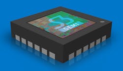
2. Depicted is a chip from S3 Semiconductors.
Design houses like S3 Semi not only develop hardware, but they can also work with customers to support the development of software for the complete system. In comparison, it’s likely that an off-the-shelf solution will only be offered with the software needed to support that component, leaving the customer to handle the system-level integration.
9. Customers are forced to use the foundry, packaging, and testing house dictated by your design partner.
This depends on the design house, but good design houses will have relationships with multiple tier 1 foundries, package, and test houses. While the design house may often want to select the best partners, customers aren’t restricted in the manufacturing partners they choose to work with. The decision is usually gated around the technology node needed to develop the custom ASIC and the cost structures being targeted.
10. Custom silicon only benefits very specific or unique niche requirements.
Custom silicon provides a wide variety of benefits for a range of industries, from improved energy efficiencies to space savings, BOM cost reductions, and IP security. Even relatively “generic” applications looking to optimize on these factors can stand to benefit.
11. Design happens in a “black box” and the customer is kept in the dark.
A good design house will work side by side at every step of the way with the customer to achieve the desired system. Rather than a black-box approach, the whole process is open and transparent.
For example, when working with S3 Semi, the discovery and development stage of the custom ASIC process is very open and transparent. Each ASIC customer has a program manager who liaises with them and the design team, to ensure there’s information exchange throughout. These discussions aren’t only focused on the current product being defined, but also look at future roadmaps.
S3 Semi believe it’s important to consider what the customer’s customer may want or need, and use this information to evaluate what can and should be done to make the customer’s solution futureproof. The company provides full information on the solution recommended, from its design and the process that will be used, to the packaging and test. And it’s important to appreciate that after all of this, the customer owns the end solution.
Edel Griffith is Technical Marketing Manager at S3 Semiconductors.
Reference:
“The Compelling Economics for OEMs to Commission their own Semiconductor Chips,” S3 Semiconductor white paper.


