High-Density Applications Demand Precision Analog Devices in Tiny Packages
Download this article in PDF format.
Traditionally, the packaged integrated circuit (IC) has been much larger than the IC itself because standard packages must also contain the lead-frame and bond wires. That wasn’t an issue for decades because space wasn’t an issue in most applications, but more recently, a couple of trends have been driving precision analog devices toward smaller packages in sizes that approximate the size of the dies themselves.
Most obvious is the move toward smaller size in the end equipment. Equipment that used to have its own room became portable and even wearable. These space-constrained applications are enough to drive a manufacturer of standard analog devices such as op amps, analog-to-digital converters (ADC), or digital-to-analog converters (DAC) to offer them in smaller packages. But new applications are also spurring the development of products that pack multiple channels into a single tiny device: so-called “high-density” products.
Take the internet, for example. Its backbone is a high-speed optical-fiber network that must continually be upgraded to satisfy the never-ending demand for increased bandwidth. New optical switching technologies such as the reconfigurable optical add-drop multiplexer (ROADM) and wavelength selective switching (WSS) technology are helping to drive throughput increases at network switching nodes. However, a WSS system requires massive arrays of DACs to help route signals between arrays of optical fibers.
Sponsored Resources:
- Second-sourcing options for small-package amplifiers
- How our DACs power laser drive applications
- Small size for big designs
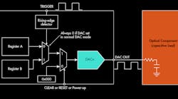
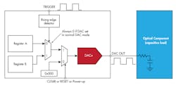
The DACs operate as square-wave generators at different amplitudes. Each DAC is configured with a high and low code; an external trigger signal toggles the output between the two codes. This function is repeated hundreds of times over many settings in any one system—thus the need for extreme integration. These systems are always space-constrained, so the more DACs per package, the better. Figure 1 shows a single DAC in a WSS system.
1. The WSS is one application that requires high-density analog components. (Source: TI E2E Blog: “96 DAC channels in one device! Why would we do that?”)
Memory testers, pin-driver circuits in automated test equipment (ATE), programmable logic controllers (PLCs), and closed-loop control are other applications that call for high-density DACs.
High-Density DACs from Texas Instruments
Texas Instruments has a portfolio of more than 40 high-density DACs. Resolutions range from 8 to 16 bits with feature sets suitable for a wide variety of applications in industrial automation, test and measurement, and optical networking.
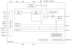
The new DACx1416, sampling now, is a pin-compatible family of 16-channel DACs with 16-, 14-, and 12-bit resolutions that comes in a 40-pin VQFN package measuring 6 × 6 mm. The family features high-voltage outputs up to ±20 V in bipolar mode and +40 V in unipolar mode. The DACx1416 (Fig. 2) includes output buffers that can sink or source up to 25 mA, reducing the need for external op amps.
2. The DACx1416 includes features that reduce solution size by minimizing the addition of external components. (Source: TI Products—Precision DACs: DAC81416)
For maximum channel count in a design, consider the 12-bit DAC60096 with 96 channels. It’s available in a 196-pin NFBGA package measuring 15 × 15 mm. Read more about the thinking behind the part here.
High-Density ADCs
The action isn’t just restricted to DACs. High-density ADCs are required for applications such as PLC modules, vibration/modal analysis, acoustics, spectroscopy, or acquiring data from strain-gauge or pressure-sensor arrays.
TI’s portfolio of high-density ADCs includes the ADS1274/ADS1278 series of 24-bit, delta-sigma (ΔΣ) ADCs with data rates up to 144 ksamples/s. These ADCs allow the simultaneous sampling of four (ADS1274) or eight (ADS1728) channels and are offered in identical packages for drop-in expandability.
Some high-density solutions include both DACs and ADCs. The AMC7832 analog monitor and control IC, for example, bundles 16 12-bit DACs, a 21-channel 12-bit ADC, eight general-purpose input/output (I/O) ports, and other functions. Target applications include communications infrastructure (base stations, microwave backhaul, optical networks); data-acquisition systems; and general-purpose monitor and control. The AMC7832’s 64-pin HTQFP package measures 12 × 12 mm.
Layout Tips for Tiny Packages
A precision DAC or ADC in a chip-scale or other tiny package requires the designer to pay careful attention to layout. This list provides some insight into good layout practices.
- Bypass all power-supply pins to ground with a low-ESR ceramic capacitor with an X7R or NP0 dielectric. A capacitance of 0.1 to 0.22 µF is recommended.
- Place bypass capacitors for the power supplies and voltage reference close to their respective pins to minimize inductance and optimize performance. Use high-quality ceramic capacitors (type NP0 or X7R) for their optimal performance across temperature and very low dissipation factor.
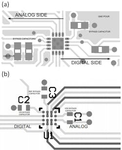
- The digital and analog sections must have proper placement with respect to the digital pins and analog pins. The separation of the two blocks minimizes coupling into neighboring blocks, as well as any interaction between analog and digital return currents. Figure 3 shows recommended layout examples for the DAC80508 octal DAC, discussed further below.
3. Comparison of DAC80508 layouts for the QFN (a) and DSBGA (a) packages. (Source: TI “DACx0508 Octal 16-, 14-, 12-Bit, SPI, Voltage Output DAC with Internal Reference” PDF)
Don’t Forget the Supporting Cast
Of course, in a real-world design, it’s not enough to have dense data converters. You also need tiny supporting circuits such as passive components, transistors, op amps, and others.
Passive components are now available in surface-mount packages down to a case size of 0201—that’s 0.6 × 0.3 mm—but a resistor in that package can only dissipate 50 mW. Ceramic capacitors in the same size are available up to 2.2 µF with an X5R dielectric, and smaller sizes are available.
MOSFETs are shrinking, too. Consider the CSD13381F4 and CSD23285F5. These 12-V devices are part of TI’s FemtoFET family of devices optimized for minimum footprint; the parts use a land-grid-array (LGA) package—a chip-scale package with metallized pads instead of solder balls. The n-channel CSD13381F4 measures 1.0 × 0.6 mm (0402 case size) and the p-channel CSD23285F5 measures 1.53 × 0.77 mm.
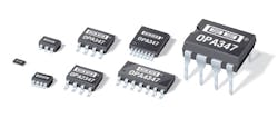
Not to be left out, op-amp manufacturers have repackaged their existing products into smaller packages to meet market demand. The 20-year-old OPA347 family (Fig. 4) is a good example. This micropower op amp has added numerous packages over the years. The dual OPA2347, for example, is available in SO-8, SOT23-8, and a chip-scale WCSP-8.
4. As the demand increases for smaller devices, many op amps have been repackaged to reduce their size. (Source: TI “microPower, Rail-to-Rail Operational Amplifiers” PDF)
Newer devices, of course, omit the larger sizes—very few PDIPs these days! TI’s new OP1671 has only one option: a 5-pin SC-70 package measuring 2 × 2.25 mm.
One concern when switching to a new package is that it may not be second-sourced, leading to production problems if there’s a shortage of the preferred part. Fortunately, many op amps adhere to an industry-standard pinout, so one solution is to modify the PCB layout to include two different op-amp package footprints to provide a second source.
The second layout is a commonly used, industry-standard package footprint that encompasses the original package. Figure 5 shows the standard pinout for a dual op-amp version and an example of a possible dual layout. Of course, this technique will increase the PCB footprint. For minimum impact, the second-source package should be as close in size to the original as possible, while maintaining sufficient space between the two sets of pads.
5. Laying out two packages for the same pinout can provide for a second source. (Source: TI Analog Design Journal “Second-sourcing options for small-package amplifiers” PDF)
Read more about the design implications of this concept in this article from TI’s Analog Design Journal.
Design Example: Precision Current Source for Laser Diode Drivers
Here’s a design example that shows how several small packages combine to produce a solution suitable for the most space-constrained applications.
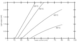
As we’ve seen, optical networks require a high channel count. Laser diodes in optical networks need a precisely controlled current to regulate their output power. As Figure 6 illustrates, the light output of a laser diode is a function of both current and temperature; maintaining the desired output over temperature requires the current to be adjustable. A microcontroller driving a DAC can be used to vary the forward current dynamically.
6. The light output of a laser diode is highly temperature-dependent. (Source: Newport)
The laser diode requires tens or hundreds of milliamps of drive current, but there are few suitable current-output DACs at this level. Thus, a voltage-output DAC plus a voltage-to-current (V/I) converter is often used instead. The drive circuit must be low-noise to reduce the intensity noise (instability in the output power) of the laser output.
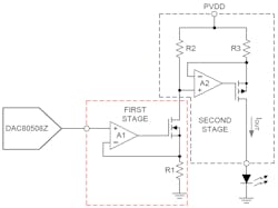
7. This laser-diode drive circuit uses a controllable current source. (Source: TI: “High-Density DACs Offer Superior Noise and Accuracy Performance in Laser-Drive Applications” PDF, p. 1)
Figure 7 shows a suitable circuit with a voltage-output DAC and a two-stage V/I converter. In the first V/I stage, op amp A1 creates a current equal to VDAC/R1 through the n-channel MOSFET; the second stage is a precision current-mirror that amplifies the current with a gain set by R2/R3. As the voltage across R2 and R3 is ideally the same, R3 < R2 to achieve the desired current gain. The output current IOUT is given by:
IOUT= (VDAC /R1) x (R2/R3)
Minimizing the value of supply voltage PVDD reduces power dissipation across the second-stage P-channel MOSFET.
There are several potential sources of error in this circuit, including:
- Gain, offset, and linearity errors in the DAC
- Stage 1 reference-current inaccuracy caused by R1 inaccuracy
- Mismatch of resistors R2 and R3, giving a V/I stage 2 gain error
- Input offset errors in the op amps creating an output-current offset
Gain errors from discrete resistors form a major part of the total error. High-precision resistors should be used, or a calibration method should be implemented. Fortunately, a simple two-point calibration can compensate for both the gain and offset errors.
The output noise of the circuit will directly impact the output power of the laser diode. Noise sources include the DAC voltage reference, thermal noise from the DAC internal resistor ladder, thermal noise from external resistors, and op-amp noise. The DAC noise sources are gained up through the V/I stage, so they’re generally the primary contributors to the total.
In this example, the eight-channel DAC80508ZYZT and an OPA2376AIYZD dual op amp feature high performance in small packages. The parts combine with two FETs from the FemtoFET family to make an extremely dense solution.
The DACx0508 is a pin-compatible family of low-power, eight-channel DACs with 16-, 14, and 12-bit resolutions and buffered voltage outputs. The DACx0508 includes a 2.5-V precision internal reference with an initial accuracy of 5 mV and low drift of 2 ppm/°C(typ.) for the DAC80508 and 5 ppm/°C (typ.) for the other device, eliminating the need for an external precision reference in most applications.
The DACx0508 operates from a single 2.7- to 5.5-V supply, is monotonic, and provides ±1 LSB integral nonlinearity (INL) performance. The devices communicate via a 4-wire SPI-compatible serial interface at up to 50-MHz clock rate, and come in two tiny 16-pin packages: a die-size ball-grid array (DSBGA) package that measures 2.4 × 2.4 mm and a slightly larger WQFN package that measures 3.0 × 3.0 mm.
The OPAx376 low-noise op-amp family incorporates TI’s proprietary “e-trim” trimming technology to minimize input offset voltage and input offset voltage drift. The part features rail-to-rail input and output (RRIO), a maximum offset of 25 µV, low noise of 7.5 nV/√Hz, a maximum quiescent current of 950 µA, and a bandwidth of 5.5-MHz.
8. Shown are the relative sizes of the components in the design example. (Source: TI: “High-Density DACs Offer Superior Noise and Accuracy Performance in Laser-Drive Applications” PDF, p. 2)
The OPA2376AIYZD is offered in several packages: the DSBGA is the smallest, at 2.3 × 1.3 mm. The resistors are 0402 (1 × 0.5 mm). Figure 8 shows the relative size of the components used in the circuit. A single channel requires a single DAC channel (1/8 of a DAC80508), one OPA2376, one CSD13381F4, one CSD23285F5, and three resistors. In a 32-channel implementation, these components take up an area of 224 mm2, slightly less than a dime. Find more about the laser-diode driver design in this application note.
Sponsored Resources:
