Download this article in PDF format.
What every RF design engineer needs these days is a good all-purpose IC RF amplifier. You don’t want to have to design basic circuits like this yourself. Yet the need is always there for a gain block you can drop into transmitters, receivers, test gear, or other projects. Fortunately, you have multiple choices these days. Here are the features you should look for when comparing RF amplifiers before buying.
Sponsored Resources:
- Working to Achieve 5G Expectations
- IDT RF Product Benefits Overview
- High-Gain Broadband RF Amplifier 600MHz to 4200MHz
Many Applications
General-purpose RF amplifiers are needed in virtually all wireless designs. Below is just a sample of the broad usage:
- 4G FDD and TDD base stations
- 5G base stations
- Wireless repeaters
- Distributed antenna systems
- Infrastructure point-to-point radios
- Public safety wireless equipment
- Military radios
- Test and measurement equipment
It’s possible to stock one RF amplifier that can fit into any signal chain of these categories.
RF Amplifier Specifications
These are the features and specifications to consider in selecting an all-purpose linear RF amplifier.
Frequency range: The broader the better for an all-purpose part. Most designs are in the 500-MHz to near 5-GHz range to cover most applications.
Gain: This depends on the application, but something in the 10- to 20-dB range is useful. And you want that gain to be the same over a wide frequency range. In most RF amplifiers, the gain will vary somewhat over a wide frequency range. Look for an amplifier with gain flatness over segments over a ±100-MHz range that’s as low as possible, less than about ±0.2 dB.
Input/output impedance: 50 Ω, of course. A must standard impedance spec for most RF signal chains.
Noise figure: Noise levels are high at these high frequencies. So, noise figure (NF) is usually critical. Remember that NF is a measure of how much noise the amplifier produces. It’s the ratio of the signal-to-noise (S/N or SNR) ratio of the amp input to the signal-to-noise (S/N or SNR) ratio of the amp output expressed in dB.
NF = 10log (SNR in/SNR out)
A signal chain that adds no noise would have a 0-dB NF. Anything less than about 3 dB is good at these frequencies; the lower the better. Seek out 2 dB as a goal.
Output power: This is the maximum power output possible with a 50-Ω load at the highest supply voltage. It’s usually given in dBm, referenced to 1 mW. The typical range is typically 12 to 28 dBm.
Third-order intercept and 1-dB compression points: The third-order intercept (IP3) and 1-dB compression (P1dB) points are measures of the linearity and efficiency in an amplifier used for power gain. With most wireless standards using OFDM, CDMA, or some other broadband modulation scheme, good linearity is essential for maximum retention of the data details and best bandwidth usage.
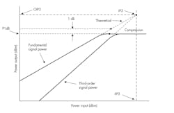
As you increase the input power to an amplifier, its output power will rise linearly. At some point the output will begin to flatten or compress, indicating distortion is occurring. The output power at which the gain has dropped by 1 dB from the linear theoretical value designates the output P1dB measurement (Fig. 1).
1. A plot of output power vs. input power showing compression, the P1dB point, and the third-order intercept point along with the IP3 at the input and output.
The IP3 figure is determined by applying two closely separated frequencies or tones to the amplifier and noting any nonlinear mixing of the tones that indicates intermodulation distortion (IMD). The tones mix to develop sum and difference frequencies along with products based on related harmonics. These are measured and plotted. The third-order products (TOPs) tend to be the most detrimental.
The IP3 is an imaginary point where the main first-order and third-order power plots meet (Fig. 1, again). It’s an indicator of how large a signal the amplifier can process before intermodulation distortion occurs. The higher values indicate less IMD. Note that you can designate the TOPs at the output (OIP3) or the input (IIP3).
Solid-state technology: Amplifiers at these high frequency ranges can be made of CMOS silicon, but more likely they’re made with gallium arsenide (GaAs) or silicon germanium (SiGe). SiGe is generally the more reliable of the two. These compound semiconductors generally perform better than silicon at the higher frequencies.
DC power: Most IC RF amplifiers operate from a supply voltage in the 1.8- to 6-V range. Current levels vary with supply voltage and the power generated and can range from 20 mA to over 100 mA. If the amplifier has a standby or low-power mode, current level should drop to no more than a few milliamps.
Packaging: Virtually all available amps are surface-mount in tiny packages. DFN and SOT-89 are common, but others are used. Sizes range from 5 × 5 mm down to 2 × 2 mm.
Temperature: Most cover the range from −40°C to +85°C or +105°C.
A Representative Example
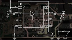
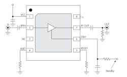
To illustrate this, consider IDT’s F0424 RF amplifier. It’s typical of what’s available in a generic broadband amplifier and one that meets the specs given earlier. It covers the 600-MHz to 4.2-GHz range. Figure 2 shows the device and its basic connections. External resistors set the bias levels, and dc blocking capacitors are employed at the input and output. The STBY pin is used to put the amplifier into a low-power standby mode when a positive voltage is applied. The F0424 is designed to operate from a heavily bypassed 3.3- or 5-V supply.
2. Here’s a simplified application of the IDT F0424 RF amplifier showing bias resistors and input/output blocking capacitors. A positive logic voltage on the STANDBY input puts the amplifier into a low-current mode.
The critical specifications are a NF of 2.3 dB, a gain of 17.3 dB, an OIP3 of +40 dB, and P1dB of 21 dBm—all at 2600 MHz. The OIP3 and P1dB values used 5-MHz tone separations also at 2600 MHz. Gain flatness over a ±100-MHz range is generally within ±0.1 dB at that same frequency. The package is a 2 x 2 mm DFN.
Sponsored Resources:


