Download this article in PDF format.
Logarithmic amplifiers with their log functionality are useful for compressing wide dynamic-range signals whereby the measured quantities are in decibels (dB). They’re used in a wide variety of applications, such as video, medical, and test-and-measurement systems. Logarithmic amplifiers can be built to be compact, easy-to-use, and cost-effective circuits suitable for certain analog designs.
Because of the high-voltage presence in industrial applications, it’s necessary to protect equipment and personnel operating the motors using galvanic isolation. Here, HCNR201/200 analog optocouplers, developed by Broadcom, can be used for current sensing and voltage monitoring in motor-control drives, switching power supplies, and inverter systems.
HCNR201/200 devices are commonly added to isolate the analog signal in the front-end module of an application’s circuitry. The optocoupler will be placed between the analog input and the analog-to-digital converter (ADC) to provide isolation of the analog input from the mixed-signal ADC and other digital circuits (Fig. 1).
1. The optocoupler is placed between the analog input and the ADC to provide isolation of the analog input from the mixed-signal ADC and other circuits.
Isolation using these optocouplers will protect the control part (such as the MCUs) from the high-voltage side of the IGBTs, if the motor-drive IGBTs are malfunctioning.
The HCNR201/200 high-linearity optocouplers are well-suited for isolating analog signals in applications that require good stability, linearity, bandwidth, and low cost. The HCNR201/200 consist of one LED and two closely matched photodiodes (PD1 and PD2).
The important parameter for the HCNR201/200 is transfer gain—it determines how closely matched are the two photodiodes. HCNR201 has a tighter transfer gain of 5%, while the HCNR200’s transfer gain is 15%. With the tight transfer gain governed by the photodiodes, the optocouplers virtually eliminate the nonlinearities and drift characteristics of the LED, with HCNR201 achieving 0.07% nonlinearity over temperature.
An example of an isolated gain amplifier circuitry using the HCNR201/200 is illustrated in Figure 2. The HCNR201/200 is connected in photovoltaic mode, as the voltage across the photodiodes is essentially 0 V.
2. This isolated gain amplifier circuitry uses the HCNR201/200 in photovoltaic mode.
The bipolar input voltage circuit in Fig. 2 uses either two HCNR201 or HCNR200 optocouplers (U1 and U3). The top half of the circuit, which consists of photodiode U1B, R1, D1, C5, R5, and LED U1A, is for the positive input voltages. The lower half of the circuit, which consists of photodiode U3B, R3, D2, C9, R4, and LED U3A, is for the negative input voltages.
Diodes D1 and D2 help reduce crossover distortion by keeping both amplifiers active during both positive and negative portions of the input signal. Balance control VR2 at the input can be used to adjust the relative gain for the positive and negative input voltages. Gain control VR1 can adjust the overall transfer gain of the amplifier. Capacitors C5, C6, and C9 are the compensation capacitors for stability.
K3 is the transfer gain of HCNR201/200.
where IPD2 is the current flowing through photodiode PD2, and IPD1 is the current flowing through photodiode PD1.
Therefore, if R1 + VR2 = R6 + VR1, then the gain of the amplifier will be unity and the output signal will follow the input signal.
Logarithmic Generator
For applications involving signals with large dynamic range, it’s difficult to deal with both small and large amplitude signals. Thus, it will require a log amplifier for signal compression.
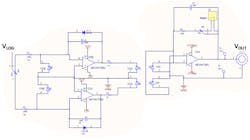
A simple circuit for a logarithmic function generator is shown in Figure 3. The circuit is built with a pair of matched transistors (Q1 and Q2) and op amps. Q1 and Q2 will serve as the feedback element for the inverting op amp. The circuit output, VLOG, is the logarithmical value of the input signal, VIN.
3. Logarithmic amplifier circuitry with VIN as the input voltage and VLOG as the logarithmic output voltage.
With Zener diode LM329, the collector current for Q2 is fixed, and, therefore, VBE2 is fixed. Only VBE1 will be affected by VIN.
Output voltage VLOG is proportional to the difference in the base emitter voltages of Q1 and Q2:
For different collector currents at Q1 and Q2, the VBE difference is governed by:
Substituting Equation 6 to Equation 5, with a difference of VBE2 and VBE1 as ΔVBE:
The ICQ1 and ICQ2 equations are:
Substituting Equations 8 and 9 into Equation 7:
With the VZ of LM329 = 6.9 V, and R5 = 681 kΩ, R1 = 10 kΩ. The logarithmic amplifier circuit gain is set by the R3 and R4 divider, (R3+R4)/R4 to a factor of 1 V/decade.
kT/q is equal to 0.02568 V at a room temperature of 25°C, where k is the Boltzmann’s constant (1.38064852 × 10⁻²³ m2∙kg∙s-2∙K-1), T is the temperature in Kelvin, and q is the charge of an electron (1.60217662 × 10⁻¹⁹ coulombs).
VBE1 is the base-emitter voltage for bipolar transistor Q1, and VBE2 is the base-emitter voltage for bipolar transistor Q2. ICQ1 is the collector current for bipolar transistor Q1, and ICQ2 is the collector current for bipolar transistor Q2. VZ is the Zener diode voltage.
Evaluation Board
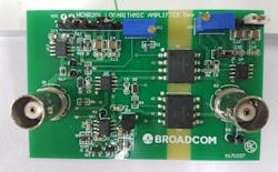
4. This evaluation board implements the isolated logarithmic amplifier using the HCNR201/200 optocouplers.
The evaluation board (Fig. 4) is built using the two HCNR201/200 optocouplers to provide isolation between the input and output circuitry.
DC Performance
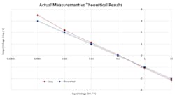
Figure 5 shows the plot of output voltage vs. input voltage for different dc input voltages ranging from 0.1 mV to 10 V. Theoretical results are computed based on Equation 6. Actual measurement results are based on the evaluation board built from the cascaded isolated and logarithmic circuits.
5. The plot shows the output voltage vs. input voltage for different dc input voltages ranging from 0.1 mV to 10 V.
AC Performance
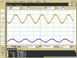
Figure 6 shows the output voltage signal (purple waveform) with a 1 V p-p ac input signal (orange waveform). The input ac signal is riding on 1 V dc. Therefore, from the plot in Fig. 3, output is with −1 V dc. Based on −3-dB cutoff frequency, the output signal is found to be at 0.5 V p-p, which is at half of the input signal. Thus, the bandwidth (-3 dB) of this circuit is 400 Hz.
6. The output voltage signal (purple waveform) is from the 1-V p-p ac input signal (orange waveform).
For ac performance, the instantaneous input ac signal level must not be less than or equal to 0 V, because the logarithmic value of 0 V and the negative input value is undefined. If an input ac signal of less than or equal to 0 V is applied, the logarithmic value will be clipped at the maximum value.
Summary
Applications for logarithmic amplifiers include digital communication systems, as well as analytical and medical test and instrumentation where safety isolation plays an important role.
These types of industrial applications measure the physical quantities over a wide dynamic range. Consequently, they use log amps to match the dynamic output to the linear input range of the signal. HCNR201/200 high-linearity optocouplers will provide the optical isolation to help ensure data integrity and to protect operators from high voltages.
Nelson Quek is Technical Marketing Engineer for Isolation Products Division at Broadcom Inc. and Robinson Law has been responsible for the application support for Broadcom's optocoupler products in industrial design-in activities.
References
“A galvanic isolated evaluation of a NTC thermistor using a logarithmic amplifier,” Yevgen Polonskiy, - Antalya, Turkey 21-24 Sept 2014.
“AN-30 Log Converters,” Application Report, Texas Instruments - May, 2013.
“HCNR201, HCNR200 High Linearity Analog Optocouplers,” Datasheets AV02-0886EN, Avago Technologies. Jul 1, 2014.
HCNR201/200, High-Linearity Analog Optocouplers Evaluation Board User’s Manual, AV02-1134EN, Avago Technologies. Apr 2, 2008.


