There has been vast progress over the last 30 years or so in digital layout automation, making it possible to develop complex digital ICs relatively quickly. However, for analog layout, techniques are still much the same as they were years ago.
True, some improvements have been made, such as using parameterized cells to generate design-rule-checking (DRC) correct primitive devices. However, placing them and carrying out power and signal routing is still largely a manual step. Electronic design automation (EDA) progress in the analog world seems to have stalled, despite the vastly increased computing power available today. There are reasons for this lack of progress.
The first is a general reluctance of analog layout engineers to approve layout generated by automated tools. When talking with layout people, even within the same company, different views are often expressed as to what is “correct.” Some form of editing the result is almost always needed, but the ability to edit the result should be done without going back to the pure polygon-level editing that most layout editors force users to adopt. The automation needs to be there, but with the ability to control and/or correct the results.
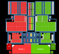
High-level editing representation of the symmetric design. The red/green coloring represents symmetrical devices; gray coloring is for dummy devices. Guard rings are shown in blue.
The second reason for the lack of progress is more complex. Digital place-and-route (P&R) using standard cells eliminates the need for complex DRC of the base layers. For analog, though, a much larger and more complex rule set must be followed if any attempt to automate the process is made—unlike DRC in the digital layout world, when only rule violations need to be detected, and then only in the routing layers.
During analog P&R, action needs to be taken to adhere to rules as the layout is formed and not having to rely on having some sort of post-layout fix-up. Modern processes have complex rules even for base layers, such as different threshold voltage devices, dummy poly, and lightly doped emitters (LDEs) making the job of the device much more complex. Concurrent electrical awareness is required to ensure that some of the more complex requirements are met.1
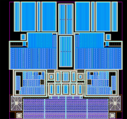
The automatically generated placed layout. At the top are PMOS devices, below are NMOS devices in deep N well, and below them are resistors and capacitors.
The ability to generate initial layout using a high-level, abstract approach means that layout engineers aren’t the only ones who can use the tool. Designers can quickly see the impact on architectural changes and device resizing without having to worry about complex polygon data or extensive submicron design rules. Then layout engineers can take over for the detailed implementation.
Therefore, a modern automated approach to speed up layout requires many considerations:
- Automatic recognition of constraints such as matching, with corresponding placement heuristics to give, for example, common centroid matched structures. Setting up constraints in some tools can take as long as implementing them manually.
- Visual interaction of constraints in both the schematic and layout domains. Circuit designers need to see them on schematics; layout engineers on the physical level.
- Rapid placement of devices and other structures like taps, dummy devices, and guard rings to produce electrically correct layout while adhering to DRC rules.
- Multiple layout choices to be generated, giving the designer a choice from which to select and carry out any detailed analysis. Using multithreading allows for the possibility of generating many floor plan candidates, unlike manual approaches where more than one layout is seldom created due to time restrictions.
- Editing capability at a high, abstract level such that structures can be moved relative to each other, but actual DRC checks happen “under the hood” to produce DRC clean layouts without the edit ßà DRC cycle of traditional polygon pusher layout tools.
- Ease of use such that circuit designers and layout engineers can generate initial layouts, and explore how architectural changes or changing device sizes (W/L/m factor/fingers) can give better matched or more compact layouts.
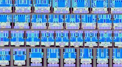
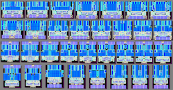
Multiple layouts are created to give a wide selection of topologies for the layout designer to choose from.
Modern Automated
Such modern tools, like Pulsic’s Animate, are now appearing in design flows and promise a significant acceleration of the layout cycle, without relinquishing the level of control required by analog designers.
Paul Clewes is Vice President of Research and Development at Pulsic.
Reference:
1. “Electrically correct Analog Layout”, Keith Sabine, Planet Analog 7th December 2016.


