MEMS Array Forms Controllable, All-Optical Photonic Switch Matrix
The tight integration of electronics and optical functions via silicon MEMS technology goes far beyond the simple combining of LEDs, phototransistors, and similar components. With the growth in links based on fiber optics, there’s a need for large, all-optical switches to route these signals across large matrices without any intervening electronics in the optical path to slow the signals, add complexity, decrease reliability, dissipate additional power, grow cost, and increase size.
To this end, a team comprising researchers at the Gwangju Institute of Science and Technology (South Korea) and the University of California at Berkeley has built a photonic switch that can control the path of optical signals faster and more efficiently than previously reported designs. Typically, existing large-scale photonic switches that control hundreds of light beams via mirrors or lenses must be physically turned to switch the direction of light. This new design uses no moving parts; instead, it electronically controls relevant characteristics of the optical path through the switch matrix.
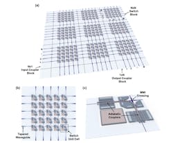
The all-optical, electronically controlled switch matrix supports 240 input and 240 output ports via a set of smaller arrays that were “stitched together” on a single wafer by design and fabrication (Fig. 1). Previous designs had a limited matrix size of 128 × 128 ports on a 1.6- × 1.7-cm die, which they note is near the maximum size available for a single reticle (usually around 2 to 3 cm for deep-UV lithography steppers or scanners).
1. Schematic of ultra-large-scale silicon photonic switches; the switch consists of the three basic building blocks: an N × N switch, an N × 1 input coupler, and a 1 × N output coupler (a). Schematic of the N × N switch block; the waveguides are tapered to a wider width to reduce stitching loss (b). Unit cell of the silicon photonic MEMS switch consisting of a pair of adiabatic couplers on orthogonal bus waveguides with MMI crossing (c). (Source: University of California)
To overcome the reticle size limit, identical switchblocks were combined lithographically with an interface loss of less than 0.004 dB, making the aggregation nearly invisible. The team built their 240 × 240 switch on a 4- × 4-cm die by stitching together a 3 × 3 array of 80 × 80 switch blocks.
The ultra-large-scale silicon photonic switches were fabricated using the 6-in. (150 mm) wafer-processing facilities in the Marvell Nanofabrication Laboratory at Berkeley. The MEMS switching element is built up from orthogonal bus waveguides with multimode interference (MMI) crossing on the first layer and a pair of vertically actuated, adiabatic optical couplers on the second layer.
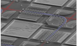
In this design, each optical element functions somewhat analogous to a microscopic highway overpass (Fig. 2). When the switch is off, the light passes straight through a lower channel (red lines). Turning the switch on changes the optical characteristics of the channel, effectively directing the light to an upper channel to make a right turn (blue lines), then a second ramp directs the light back down.
2. Each individual “light switch” is constructed like a microscopic highway “overpass” such that when a switch is off, the light passes straight through a lower channel (red lines). Turning the switch on lowers a tiny ramp that directs the light to an upper channel so that it makes a right turn (blue lines), where a second ramp lowers the light back down. (Source: Tae Joon Seok)
[Note: An adiabatic optical coupler is unrelated to adiabatic processes in thermodynamics. Here, it’s a theorem in quantum mechanics, proposed in 1928. It says that a quantum-mechanical system, including photons, which is subject to gradually changing external conditions will change and adapt its functional form. However, when the system is subject to rapidly varying conditions, there’s insufficient time for the functional form to adapt, so the spatial probability density of the particles remains unchanged. By comparison, an adiabatic process in thermodynamics occurs without transfer of heat or mass of substances between a thermodynamic system and its surroundings. The References below provide further insight on the mechanics—quantum and fabrication—of adiabatic coupling.]
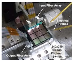
Testing required a custom arrangement as well (Fig. 3). To characterize the switch, a measurement setup was built with two motorized six-axis stages to align the two fiber arrays with the input and output coupler blocks. Two 80-channel fiber arrays with 13-deg. polishing angles were used to interface with the switch. With this setup, the team could probe any 80 × 80 switch blocks by moving the fiber arrays along the input or output couplers.
3. The experimental setup with the 240 × 240 silicon photonic switch shows the coupling of the input and output fiber arrays as well as the arrangement of test probe. (Source: University of California)
To minimize losses due to physical-alignment mismatch at transitions between the various internal MEMS optical waveguides, the ends of each such path were precisely tapered; the on-chip loss is just 0.04 dB/port. The multilayer adiabatic-coupler switch with MEMS actuation offers many advantages, both in theory and as demonstrated by tests on the fabricated device: zero loss in the OFF state; low propagation loss; extremely high on/off extinction ratio (>60 dB); low crosstalk (better than −60 dB) over a broad wavelength range (>100 nm); and a switching time of under 400 ns.
The researchers believe that what they have devised and assessed is both the largest integrated photonic switch ever reported, and with the lowest on-chip loss per port. Their full paper, “Wafer-scale silicon photonic switches beyond die size limit,” and “Supplementary Material” published in the journal Optica from the Optical Society of America provides in-depth detail on the principles, implementation, and tests of this UC Berkeley project. The research was funded by the Advanced Research Projects Agency–Energy, the National Science Foundation, Google Faculty Research Award, UC Berkeley Bakar Fellows Program, and the National Research Foundation of Korea.
References
IBM Research Lab (Zurich), “Scalable Optical Coupling between Polymer Waveguides and a Silicon Photonics Chip”
arXiv.org, “Shortcut to adiabatic light transfer in waveguide couplers with a sign flip in the phase mismatch”
American Institute of Physics, APL Photonics, “Adiabatic mode converters for silicon photonics: Power and polarization broadband manipulators”
Wikipedia, “Adiabatic theorem” (quantum physics)
Wikipedia, “Adiabatic process” (thermal)


