Clean and Thin Are In: 2D Transistors Get Closer to Reality
Two-dimensional semiconductors measuring just a few molecules thick have a number of valuable properties that could be used to create novel electronic devices. However, creating such components with good contacts and stable performance has proved challenging (this is somewhat reminiscent of the challenges in developing the ohmic contacts for early geranium transistors in the 1950s).
Now, a research team at the Columbia University School of Engineering and Applied Science (SEAS) has developed a technique that overcomes the contact problem. Transistors (FETs) are made using a two-dimensional (2D) material stack with a semiconducting layer that's only two atoms thick, yet has both high yield and consistent performance (Fig. 1).
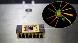
1. This enhanced optical microscope image shows a Hall-bar structure used to characterize transistor properties for devices made with ultraclean transferred contacts. The long radial lines, made from deposited gold, connect the small contacts at the center of the device to large probe pads for easier access and measurement. (Source: Columbia University)
The group was trying to create transistors out of transition metal dichalcogenides (TMDCs), but multiple attempts to make devices on tungsten diselenide (WSe2) with a variety of different metal contacts yielded very poor results—either very low currents or no current at all. Even for those devices that did work, performance would often degrade even while being measured, which was extremely frustrating. The team believed that this initial poor performance or subsequent degradation was due to dirt and damage on the conventional via contact that occurred during lithography and metallization.
Lead researcher Prof. James Teherani noted, “The thinness of these semiconductors is a blessing and a curse….While the thinness allows them to be transparent and to be picked up and placed wherever you want them, the thinness also means there's nearly zero volume—the device is almost entirely surface. Because of this, any surface dirt or contamination will really degrade a device.”
To solve the problem, they decided to leverage results from other researchers who used full hexagonal boron nitride (hBN) encapsulation of graphene devices. After several false starts (discussed in the paper) they embedded metal in a top hBN encapsulation layer and then transferred this layer onto the semiconductor channel, thus creating a fully encapsulated semiconductor device structure with topside contacts. This would ensure that the “dirty” steps of the process (etching, electron beam lithography, and metallization) would be completed away from the semiconductor, hopefully allowing its surface to remain pure and clean.
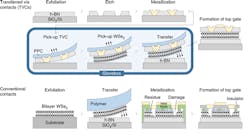
However, the results were still poor when they transferred the via contacts in air. So, they tried an alternative approach of using glove box processing of the WSe2 flake to reduce hysteresis and variability across the contacts. They repeated the device fabrication, but this time with all steps involving WSe2 performed inside a purged, nitrogen-filled glove box, which significantly improved results for the transferred via contact (TVC) devices (Fig. 2).
2. The fabrication process for transferred contacts (including the glove-box steps) yielded nearly ideal transistors. The technique prevents prevent contamination of the transferred contacts and damage to the 2D semiconductor that occurs during fabrication of conventional contacts. (Source: Columbia University)
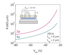
The FETs they created from bilayer p-type WSe2 showed high hole mobility and low contact resistance, as well as high current and stability for over two months of measurements. In addition, the low contact resistance and clean channel allowed for the creation of a nearly ideal top-gated p-FET with a subthreshold swing of 64 mV per decade at 290 K (Fig. 3).
3. Two-probe (2p) and four-probe (4p) measurements of TVCs were performed on bilayer WSe2. The width-normalized resistance is plotted as a function of back-gate voltage (VBG) at room temperature. In the 2p measurement, the voltage is sourced across contacts 1 and 4, and current is measured across the same contacts: R2p = W × VDS/ID. In the 4p measurement shown in the inset, the voltage is measured between terminals 2 and 3 to eliminate the impact of contact resistance: R4p = W × V23/ID. The contact width is 6 μm. (Source: Columbia University)
Details of the project are presented in their Nature Electronics paper “Transferred via contacts as a platform for ideal two-dimensional transistors.” They also mounted the devices in a chip carrier (Fig. 4) for extensive electrical characterization of the device at both low temperatures and high magnetic fields using a cryostat with a tunable magnetic field. The results of these tests, as well as others not covered in the basic paper, are in their Supplementary Material.
4. A Hall-bar device structure (see inset) is wire-bonded to a 16-pin chip-carrier, which then allows for extensive electrical characterization of the device at both low temperatures and high magnetic fields. (Source: Columbia University)
The team concluded that transferred via contacts made from metal embedded in insulating hexagonal boron nitride and dry transferred onto 2D semiconductors can create high-quality 2D transistors. This approach prevents the damage caused by direct metallization by providing a clean, stable, and damage-free platform for 2D device fabrication. Prof. Tehrani explains the step-by-step process of the dry transfer process used to create ultraclean stacks of 2D materials in this four-minute video:
(A short preceding video “Building at the Nanoscale | Part 01: 2D versus 3D Materials” is for a non-technical audience.)
