Tailoring the Design of Transimpedance Amplifiers to Infrared Sensor Apps (Part 1)
What you’ll learn:
- How transimpedance amplifiers are used in fiber-optic communications, laser rangefinders, and LiDAR systems.
- How avalanche photodiodes enhance TIA performance.
- Application-specific design and topology considerations for TIAs.
The performance requirements of transimpedance amplifiers (TIAs) vary significantly between applications. In high-speed communications, wide bandwidth is important, creating challenges in designing for high stability. In most applications, noise performance is critical to overall system sensitivity, and gain requirements vary.
Large-area photodiodes present higher input capacitance, which may require the design of compensation circuits, and environmental considerations include the ability to maintain acceptable performance over a wide range of temperatures. Size, power consumption, and cost are other ever-present issues. Part 1 considers TIA performance priorities and tradeoffs for two of the three applications discussed in the series: laser rangefinders and LiDAR systems.
TIAs for Optical IR Sensors
Optical infrared sensors are ubiquitous, finding homes in many applications such as motion and proximity sensing, gas and particle sensing, spectral analysis, optical communications, and test. While the optical-to-electrical conversion is typically done by a photodiode, another key function of any infrared sensor is the signal conditioning of the output photocurrent into a useful signal that can be processed downstream.
In this first stage of signal conditioning, a transimpedance amplifier (TIA) converts the photocurrent into an output voltage swing right across the required dynamic input range of light incident on the photodiode. For this article, we will consider a specific type of photodiode called the avalanche photodiode (APD) that’s used to detect very low levels of light and thus is particularly suited to laser rangefinders (LRFs) and LiDAR systems.
What is a TIA?
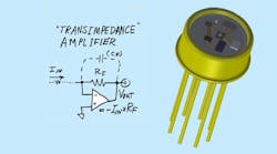
A transimpedance amplifier is a current-to-voltage converter, usually implemented with one or more operational amplifiers. The TIA also amplifies the signal from the photodiode to a usable voltage. It presents a low impedance to the photodiode and isolates it from the output voltage.
In its simplest form, a TIA has just a large-valued feedback resistor (Rf). The closed-loop gain of the amplifier is set by this resistor. Because the amplifier is in an inverting configuration, it has a value of −Rf, if the amplifier's open-loop gain is large enough.
There are several different configurations of transimpedance amplifiers, each suited to a particular application and the characteristics of the preceding photodiode. The one factor they all have in common is the requirement to convert the low-level current of a sensor to a voltage.
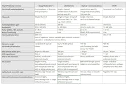
Some key factors common to TIAs for all three applications are photodiode capacitance, system gain/bandwidth, and noise. Other considerations include the overload or saturation requirements, the interface between the photodiode and TIA, the target optical sub-assembly package being used, the voltage output signal needed to interface with the next processing stage, and external environmental factors such as ambient light or reflections (see table).
TIAs for Laser Rangefinder Applications
Laser rangefinder applications use a high-power laser source to “fire” pulses of light at objects in the line of sight. The reflected light is then captured using the APD receiver and processed to calculate the distance to the object.
Typically, LRFs use a single transmitter and receiver component; therefore, only a single TIA circuit is needed. The laser light pulses are typically in the order of 1 to 100 ns in duration, which results in a TIA bandwidth requirement in the order of hundreds of MHz. Since the reflected light power can be very small, the overall transimpedance gain required to amplify small photocurrents can be in the order of 100 kΩ.
Operating with high transimpedance gain often introduces a bandwidth constraint. A noiseless APD really helps this situation because it can operate at high multiplication gains without also increasing noise, which is what usually happens with conventional APDs. High multiplication gain in the APD relaxes the TIA gain requirement somewhat, making it easier to meet both gain and bandwidth targets.
Low input noise is highly desirable for LRFs, which requires using an extremely low-noise APD coupled with a low-noise TIA design. To achieve the needed gain, noise, and bandwidth without running into stability issues with large input powers often means the TIA circuit is engineered from discrete components and widely available op-amp integrated circuits.
The APDs often operate near their device noise floor. This may require additional control of gain across temperature or even being held within a specific temperature range using a thermoelectric cooler (TEC) element—both of which add cost and complexity to the TIA interface circuit design.
Traditionally the lowest-noise TIAs have been designed using discrete transistors. However, availability and obsolescence have seen an increase in the use of op-amp ICs with additional surrounding support circuitry to tailor the TIA design for the particular application and environment requirements.
To achieve the distances required for industrial and particularly military LRF applications, the TIA is highly linear and covers a large dynamic range. Circuit techniques at both the input to the TIA, such as using a resistor or resistor-capacitor or a “dump diode,” and proceeding output gain stages (e.g., time variable gain amplifiers) are used to reduce input current and control gain. This improves the overload capability or damage threshold as well as the impulse response recovery time. External noise from ambient light incident on the APD also requires compensation techniques to reduce errors in measurement accuracy and range.
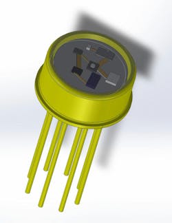
The APD and TIA are often packaged together in a dedicated receiver optical sub-assembly solution that also includes the additional circuit components and functions such as input protection, TEC, APD bias voltage control, and post-amplification. The output is usually a single-ended output that can be interfaced directly into an analog-to-digital converter (ADC) or threshold comparator (see figure).
Selecting and using an extremely-low-noise APD can help to reduce the complexity of the TIA circuit design and provide improved range performance without an increase in the required transmitter power.
TIAs for LiDAR
LiDAR implemented using the time-of-flight (ToF) method shares some similar characteristics and requirements to LRFs in terms of principle of operation, laser pulse widths, and bandwidth requirements. A key difference is the sophistication of the overall system—it’s required to scan and gather information in 2D/3D. This often requires multiple sensors to be deployed, which are based around single or array APDs interfaced to multichannel TIAs.
While single-channel TIAs can be implemented with dedicated op-amp ICs—similar to LRFs—array APDs are more likely interfaced with LiDAR application-specific integrated circuit (ASIC) TIA arrays.
LiDAR transmitters must transmit a significant amount of laser energy that’s subsequently reflected off incident objects in the scanning pathway. However, the reflected light received at the sensor can be orders of magnitude smaller than the light transmitted, so a low-noise APD with a large active area is desirable.
Such APDs are often packaged in TO-cans or SMD packages with large windows to collect as much incident light as possible, rather than the lensed package often used in optical communications. This also drives the requirement for an APD with a larger active area.
APD capacitances on the order of 2 pF are not uncommon. As a result, several challenges arise in the TIA circuit design as larger capacitance at the TIA input reduces front-end bandwidth, increases noise, and adversely affects circuit stability.
LiDAR TIAs, like LRF, must cope with incident ambient sunlight that reduces the input signal-to-noise ratio, consumes large proportions of the available dynamic range, and even saturates the TIA front end, necessitating the use of compensation circuitry. Two common methods of compensation are AC coupling and/or DC feedback correction loops, both of which have pros and cons.
However, unlike LRF, multichannel LiDAR systems can be power-hungry due to the amount of APD TIA channels deployed. This drives the requirement for specialized LiDAR TIA ASICs with power-down options for various parts of the TIA circuitry when idle but can activate quickly when in use. LiDAR ToF TIA outputs are typically amplified by a voltage driver and quantized using an ADC or time-to-digits converter.
Part 2 discusses TIAs for high-speed optical communications and design considerations and recommendations for each of the mentioned applications are made.
AndyT's Nonlinearities blog arrives the first and third Monday of every month. To make sure you don't miss the latest edition, new articles, or breaking news coverage, please subscribe to our Electronic Design Today newsletter.


