Extract the Best AC Performance from Your Precision DAC
Sometimes it seems as though digital designers get all of the attention. In all of the excitement surrounding "gigaFLOPS," "22 nm," and such, there's still one crumb of comfort for we non-digital types: the real world is—and will remain—stubbornly analog. But we still have to work with our digital friends, so...
A digital-to-analog converter (DAC) converts digital input data into an analog output. The definition of "precision" may vary between manufacturers, but at TI, we're talking about a resolution of 8 to 18 bits and a speed of up to 10 Msamples/s. These DACs are used in numerous applications: audio and video equipment; process control; RF base stations; instrumentation; automatic test equipment (ATE); closed-loop control; and many more. Each application has its own set of DAC requirements for resolution, ac and dc performance (also known as static and dynamic performance), power consumption, and so on.
Some applications like waveform generation or video displays emphasize ac performance, which is specified in the datasheet by parameters such as settling time, noise, and glitch performance. Making the most of the raw numbers in an actual application, though, is more complicated than simply perusing the datasheet, because it involves both the DAC and its external components. Read on to find out what steps you can to take to maximize your DAC’s ac performance.Applications such as motor control and process control call for excellent dc performance. This is specified in datasheet parameters such as offset error, gain error, differential nonlinearity (DNL), and integral nonlinearity (INL). Read more about DAC dc specifications here.
Three Architectures for Precision DACs
When choosing a precision DAC for your application, it's important to match the DAC specifications to application requirements. Compared to the plethora of ADC architectures, precision DACs may seem more straightforward with three main choices. However, significant performance differences exist between each one.
The three primary architectures used are the string DAC, the R-2R DAC, and the multiplying DAC (MDAC). A brief discussion of these types follows, but you can find more exhaustive treatments here and here.
String DAC
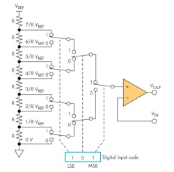
The concept behind the string DAC architecture dates back to Lord Kelvin in the mid-1800s (Fig. 1). The input decoder drives a number of switches, one for each bit combination. Each digital input code then connects a corresponding voltage to the output buffer amplifier.
An N-bit DAC consists of a string of 2N matched resistors, with the voltage reference at one end and ground at the other. The three-bit DAC shown in Fig. 1 requires seven switches and eight resistors, but these numbers rapidly increase—a 16-bit string DAC needs 65,536 resistors! Even in a world of submicron feature sizes, this is a eye-opening number. Thus, newer designs use interpolating amplifiers and tapping points on individual resistors to reduce the number of required resistors.
The string DAC is suitable for most precision applications, and finds use in dc bias control, adjustable references, or closed-loop systems such as digital servos or motor control.
The output voltage of the string DAC is inherently monotonic with good DNL performance, but its INL performance isn’t on that level since it depends on the relatively imprecise resistor matching. In terms of ac, the string DAC exhibits lower glitch performance than other DAC architectures, but its noise is relatively high due to the impedance of the resistive string array. The switching structure leads to slow code-to-code transitions, limiting the update rate.
R-2R DAC
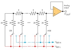
The R-2R resistor ladder is one of the most common DAC building-block structures (Fig. 2). This architecture uses resistors of only two different values, with a ratio of 2:1. Unlike the string DAC, an N-bit R-2R DAC requires only 2N resistors, vastly simplifying the task of trimming.
If a particular bit is set, the corresponding 2R resistor is switched to VREF-H; otherwise it’s connected to VREF-L (ground). The resulting output voltage is the sum of all 2R ladder voltages.
The R-2R DAC is well-suited to industrial applications. It’s more accurate than the string DAC, is lower noise due to its lower resistor couint, and has excellent INL and DNL performance.
With the R-2R DAC, each new update involves switching the 2R legs to either VREF-H or ground. The internal resistors and NMOS switches are never perfectly matched, so variations in gate-switch timing appear as a glitch at the output of the DAC after a code transition.
MDAC
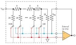
The MDAC also uses the R-2R resistor ladder, but the reference voltage VREF is at the beginning of the ladder (Fig. 3). When a bit is set, its corresponding 2R resistor is switched into a virtual ground—the summing junction of an external op amp. The MDAC, therefore, outputs a current instead of a voltage. The reference voltage VREF can exceed the supply voltage and even go negative.
The VREF pin in the MDAC sees a constant impedance equal to R, so its output current is always constant. This improves performance during fast code transitions because there’s no need to wait for the voltage reference to settle to the new current value. Depending on the digital code, the current flow divides between the output pin and the ground pin, which means there will be a varying output impedance. This complicates the selection of the external op amp.
To improve output performance, MDACs include an internal feedback resistor with thermal response closely matched to that of the internal resistor ladder. The internal noise of an MDAC comes from both the resistor ladder and the feedback resistor. Since the output impedance is code-dependent, so is the noise gain, although the MDAC noise is much lower than that of a string DAC. In addition, the external op amp can be a low-noise type, such as TI's OPA277.
One disadvantage is that the output’s polarity is opposite of the input, which in turn requires an extra inverting stage.
Understanding AC Performance Parameters
To get the best ac performance out of your precision DAC, it's important to understand the main ac specifications and what steps you can take to optimize them.
Settling Time
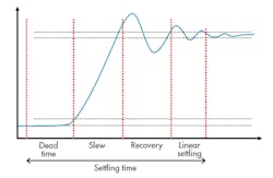
The time taken for the DAC's output op amp to settle to its final value is the largest contributor to the DAC's settling time, accounting for three of the four segments illustrated in Figure 4. The initial "dead time" is the delay due to the DAC digital interface. The four segments are defined as follows:
• Dead time: The time required for the output to rise to 10% of the desired analog output value, starting from when the digital code was applied to the DAC.
• Slew time: The time required to transition from 10% to 90% of the desired analog output.
• Recovery time and linear settling time: Initial overshoot and final stage, often referred to as large signal settling time and small signal settling time, respectively.
Once the output settles inside a predetermined error band, the output is considered to be at its final value, even though some residual setting may still occur.
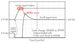
Figure 5 shows a real-world measurement with the DAC9881, an 18-bit, single-channel, low-noise R-2R DAC. The settling time is measured from when the LDAC (Load DAC) input pin goes low and allows the input data to propagate through the system. Note that the slew makes up the largest component of the settling time, with a small recovery time and insignificant contributions from the other elements.
A DAC datasheet shows the settling time under a specified set of test conditions. The DAC9881, for example, settles to 0.003% of full-scale range (FSR), driving a 10-kΩ resistor in parallel with a 50-pF capacitor. The code transitions from 0x04000 to 0x3C000, a large step size intended to be a worst-case figure. The settling time is less for smaller code transitions.
Since the op amp is the largest contributor to settling time, the best way to reduce it is to use an MDAC architecture with an appropriate external op amp. This topic is best dealt with separately; see here for more information.
Transition Glitches
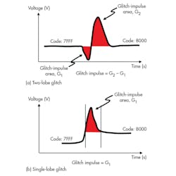
An ideal DAC changes from one output to the next monotonically, but a real-world output exhibits both overshoot and undershoot. Unlike settling time, a glitch stems from the DAC circuitry itself, being caused by mismatches in internal switching times (the dominant factor) or capacitive coupling of digital input transitions to the analog output (Fig. 6).
The glitch is characterized in terms of the area under the positive and negative glitch impulses, and is specified in volt-seconds (more commonly μV-s or nV-s).
A large number of switches changing in parallel increases the glitch—we’ve already mentioned this as one of the weaknesses of the R-2R architecture. The R-2R glitch is most noticeable when all bits change, or during the most-significant-bit (MSB) transition, when bits are switching from 0x7FFF to 0x8000 (for a 16-bit DAC). A string DAC features fewer nodes simultaneously switching and will, therefore, exhibit a smaller glitch area than an R-2R DAC.
7. Two options are available for reducing the output glitch: an RC filter (a) and a sample-and-hold circuit (b). Each option has advantages and drawbacks. (Source: TI)
If changing to a string DAC isn’t an option, Figure 7 shows two glitch-reduction techniques. Figure 7a shows a simple RC filter on the DAC output. Though easy to implement, it will not remove the glitch completely, rather only reduce its amplitude. It will also increase settling time. Another option is to add a sample-and-hold circuit (Fig. 7b). This will substantially remove the glitch, but is more difficult to implement since it imposes strict timing requirements that are synchronized to the DAC update rate.
Noise Sources
Noise is another important component of DAC ac performance. There are three major contributors to DAC noise: the internal resistor network, the internal or external output amplifier, and the internal or external voltage reference. Internal resistor noise was mentioned in our discussion of DAC architectures, but let's look at the other two.
• External Op-Amp Noise
The DAC's output amplifier is another source of noise. An MDAC uses an external op amp, but other architectures integrate the op amp internally and quote an overall noise figure. The DAC9881, for example, has an integrated output buffer with rail-to-rail operation and a noise figure of 24 nV/√Hz.
Noise in an op-amp circuit has four basic components: 1/f noise (also known as flicker noise), broadband voltage noise (white noise), resistor voltage noise, and current noise. The first two are considered intrinsic properties of the op amp itself. The bandwidth is limited in a typical DAC application, so broadband noise isn’t a significant contributor. For best ac performance, therefore, look for op amps with low 1/f noise. Find out more on this topic at TI's Precision Lab series on Noise in Op Amps.
• External VREF Noise
The noise performance of a DAC depends directly on the reference voltage, which may be internal or external. For best noise performance, a precision low-noise external reference should be used, since the noise generated by the reference couples through to the analog output.
There’s a huge selection of precision VREFs available from several manufacturers. For more information on voltage references, refer to this document on Voltage Reference Selection Basics.
Conclusion
Getting the best ac performance out of a precision DAC is a combination of understanding the specifications, picking the right architecture, adding the right external components, and, of course, following correct layout practices.
TI offers a number of aids to help in this task, including a comprehensive DAC parametric selection tool as well as training videos and DAC-related technical resources.
