This Company is “Open” to Silicon Photonics
This article is part of the TechXchange: Silicon Photonics.
What you'll learn:
- What is silicon photonics?
- The integration of lasers and amplifiers into silicon photonics.
- This year's launch of OpenLight.
Silicon photonics promises to bring higher bandwidth and lower power communications solutions for chip-to-chip and board-to-board connectivity.
OpenLight was launched as an independent company in 2022 with investments from Synopsys and Juniper Networks. It’s delivering the world's first open silicon-photonics platform with integrated lasers.
I talked with Tom Mader, Chief Operating Officer at OpenLight, to find out more about silicon photonics and his company.
For readers who aren’t familiar, what is silicon photonics, and why is it important today? How does it differ from traditional electronics?
Simply put, silicon photonics utilizes silicon to guide and process light. This uniqueness enables foundries to expand from making only electronic chips to now also producing high-volume photonic integrated circuits (PICs). The technology, which evolved from transistor-based silicon technology, has earned an early stronghold for its scale and cost advantage compared to conventional discrete photonic solutions (Fig. 1).
Overall datacom speed requirements have become high enough to benefit from the technology’s strengths. Silicon photonics allows for much higher photonic complexity than discrete designs, delivering improved performance, better power efficiency, and better cost at scale. This is more important today than ever, because of the increasing data-transfer and power-consumption requirements driving companies toward innovative ways to compute, store, and move data faster.
Tell us more about the new company and its launch. What is OpenLight?
OpenLight is a new, independent company that was formed with investments from Synopsys and Juniper Networks in April 2022 and launched officially in June of this year. Headquartered in Santa Barbara with offices in Silicon Valley, we are offering the world’s first open silicon-photonics platform with integrated lasers. Our technology and unique ability to integrate lasers on chip is at the heart of our approach to transforming the silicon-photonics industry. Our first open multi-project wafer (MPW) for customers is taping out and starting fabrication later this year.
As an analogy, we’re similar to Arm in how we function. We are a license-based royalty company providing photonic customers with a means to create high-performance PICs. We offer customers a library of photonic components as part of the Tower PH18DA process design kit (PDK) and verified PIC designs, addressing popular datacom transceiver standards, evaluation hardware samples, and design services.
What are some of the challenges that persist for designers and engineers in the industry today? How does OpenLight alleviate some of those challenges?
New technologies always come with an adoption curve and there are still large barriers-to-entry to customers. One of these barriers is the lack of on-chip lasers and amplifiers, which causes two problems. The first problem is that customers need to source lasers separately from the silicon-photonics chip, which adds supply-chain complexity. The second problem is that it’s difficult to set up the packaging infrastructure to attach lasers to silicon photonics, and it is difficult to ramp. OpenLight’s technology eliminates both issues.
Can you tell me more about the technology, including the integration of lasers and amplifiers?
OpenLight’s technology fuels the world’s first open silicon-photonics platform, which includes integrated lasers and amplifiers, based on InP (indium phosphide) bonded to silicon. This is offered through our foundry partner, Tower Semiconductor.
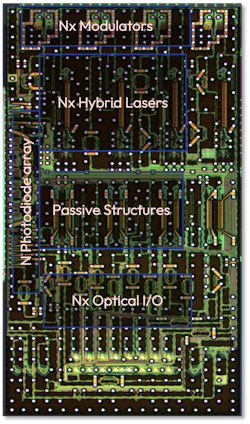
The underlying technology enables very high coupling efficiency between InP lasers and InP amplifiers and the silicon waveguides, with the ability to make photonic chips with large numbers of elements that have high yield. Processing indium phosphide directly on silicon photonics wafers not only brings a new level of scale, but also reduces losses.
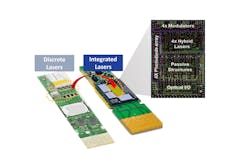
Figure 2 shows a comparison of discrete lasers versus integrated lasers in a PIC, in the context of a datacom module.
This fills the market need for an open, functionally complete PIC platform that doesn’t require expensive and power-hungry separate laser sources. We are excited to offer our platform to anyone who wants to design and create products whether they be in datacom, LiDAR, or other emerging applications.
What is the main differentiator for OpenLight?
OpenLight’s technology greatly simplifies PIC manufacturing as it enables customers to bypass separate sourcing of lasers, as well as the cost, yield, and optical loss that comes with discrete coupling of laser signals into the PIC. Moreover, the OpenLight platform enables high-complexity photonic designs with a large number of channels, lasers, and optical amplifiers on-chip. Because our lasers are produced and aligned on-chip using extremely accurate wafer fabrication methods, customers can design PICs with a large number of active components that aren’t typically feasible.
What are OpenLight’s product and expansion plans going forward?
We are currently taping out the first open MPW shuttle run on the Tower PH18DA process as well as 400G and 800G reference designs with integrated lasers. Both our PDK and our PIC designs provide access to our technology, enabling unparalleled scale, speed, power consumption, and cost-effectiveness.
For the first time, a solution is available that accelerates the development of high-performance PICs in applications such as LiDAR, datacom, telecom, healthcare, HPC, AI, and optical computing. OpenLight has an exciting roadmap of future components and PIC reference designs that we are happy to share with customers under NDA.
What industries and which geographies do you expect the most growth from initially?
One of our early market segments where we are seeing traction is the datacom market. We expect this to be one of our early growth areas. We are also seeing a lot of interest from LiDAR customers, especially those pursuing coherent architectures. In addition, there are customers from high-performance computing and AI, other sensing customers, optical computing, and, of course, telecom applications.
According to LightCounting, the market for silicon-photonics-based products is expected to increase from 14% in 2018-2019 to 45% by 2025, indicating an undeniable inflection point for the technology’s adoption. In terms of geographies, we serve customers worldwide and continue to work toward our mantra of being “open” to make our technology widely available. We’re proud to be pushing forward and helping more teams discover new possibilities with our open platform.
What challenges do you anticipate as a new silicon-photonics company?
As with any new technology offering, industry adoption requires time and effort. Customers need to familiarize themselves with new design tools and a new type of PDK that involves active optical components.
Fortunately, we offer powerful advantages to customers (scale, speed, and power consumption). These powerful advantages are generating a lot of interest and they are motivating customers to move over to our platform.
Tom Mader is the COO of OpenLight. Before OpenLight, he headed the silicon photonics division at Juniper Networks for over two years.
This article is part of the TechXchange: Silicon Photonics.


