With 14 envelope-tracking-enabled handsets now on the market, and more sets to follow in the coming years, envelope tracking (ET) has been firmly accepted as the industry standard for the architecture of 4G RF front ends. Some predictions assert that 8 billion ET solutions will ship over the next five years.
While the market case for ET may be largely accepted, designers are now focusing on how to optimize their ET solutions to deliver the best RF performance, highest data rates, and longest battery life for handsets.
This file type includes high resolution graphics and schematics when applicable.
Much has been written about the wider system-level aspects of ET, and the impact on RF power amplifier design, performance and characterization. However, relatively little has been said about the chip at the heart of this revolutionary technology—the ET power-supply modulator itself.
The engineering challenge in developing an ET chip concerns the creation of a power-supply converter that simultaneously achieves high efficiency (>80%), extremely high bandwidth (>20 MHz), very low noise, and high peak output currents (>1 A). These goals aren’t insignificant. Although simple in concept, ET is a complicated technology to get right and, perhaps unsurprisingly, there’s more than one way to “do” ET.
For IC designers, delivering an effective ET power-supply modulator requires an architecture that delivers the right balance between the key metrics—system efficiency, noise, bandwidth, and output power—while paying attention to some of the less obvious requirements, such as output impedance, slew rate, and mode transition times.
ET chips must also support fall back to traditional average power tracking (APT) operation at reduced output powers. In this scenario, they must deliver competitive efficiency and consume no more current than yesterday’s APT-only dc-dc converters when heavily backed off.
Let’s take a look at some of the insights into the technical requirements for a “good” ET supply modulator, and consider the features that provide scalability to meet future performance, integration, size, and cost requirements.
What Makes a Good ET IC?
At its simplest, ET is a very fast power-supply technique. By dynamically modulating the supply voltage in synchronization with the instantaneous amplitude, or "envelope," of the transmitted RF signal, ET can significantly improve the energy efficiency of RF power amplifiers (PAs).
To deliver optimal system performance, ET power-supply modulators must achieve a number of crucial characteristics simultaneously:
• High bandwidth
• High efficiency
• Low noise and distortion
• Wide swing range
• High slew rate
• Low output impedance
• Boost capability
• Seamless-mode transitions
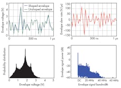
Figure 1 shows example ET waveforms for a 20-MHz (100RB) LTE uplink waveform. These provide some insight into the challenges of creating a good ET modulator.
High bandwidth
One of the main implementation challenges for an envelope-tracking IC concerns bandwidth—it’s a power supply that must accurately track the signal amplitude of the RF signal without clipping or introducing distortion. This requires a power supply with a control bandwidth of 1.5 to 3.0 times the RF channel bandwidth, i.e. 30 to 60 MHz for a 20-MHz orthogonal frequency-division multiplexing (OFDM) channel.
It can be seen from the spectral plot of the envelope signal power (lower right of Figure 1) that there’s a large dc component, followed by a significant amount of power within the occupied channel bandwidth, and then a relatively long “tail” out to at least three times the channel bandwidth. The amount of this tail that must be tracked by the ET IC depends on the system RF linearity requirements.
High efficiency across a wide range of signals
Perhaps harder than achieving the absolute bandwidth through the ET IC is to maintain high energy-conversion efficiency for the ET IC itself. While 85% ET IC efficiency remains a good figure of merit for low-bandwidth signals such as 3G, maintaining this efficiency over a wide range of signal types and bandwidths is a significant architectural and IC design challenge.
Maintaining high efficiency over a wide power-control range is also important for applications such as LTE and 3G, which employ dynamic power control. ET will usually deliver a power-saving benefit over the top 8 to 10 dB of the power-control range. In addition, as power is backed off, the ET IC’s efficiency usually determines the “break-even” point compared with APT.
ET ICs for cellular applications will also include a lower-bandwidth APT mode for operation at reduced power levels. This, too, must operate at high efficiency over a very wide power output range—from 10 mW to more than 1 W—making circuit design for low quiescent currents an important architectural and design consideration.
Low noise
In an ET system, the PA operates in compression, and power-supply noise generated in the ET path is directly “mixed” with the RF input signal. To minimize noise and distortion products at the PA output, the ET modulator must operate with an extremely low noise and distortion. If switch-mode power supply techniques are employed, it becomes a difficult problem to solve.
In frequency-division-duplex (FDD) systems with narrow duplex separation, such as the US 700-MHz LTE bands, the ET-path noise and distortion are particularly difficult to achieve.
Wide swing range
The mapping of instantaneous RF amplitude to ET supply voltage is defined digitally in the baseband by a shaping table, which can be varied to trade off efficiency and linearity of both the PA and the ET IC. The ET IC output must be able to swing over a wide (>3:1) voltage range, as a limited dynamic swing range will only deliver limited power savings in the PA.
The dynamic swing range of an ET modulator is as important as ET converter efficiency; increasing ET swing range increases PA efficiency. However, ET IC efficiency will decrease, and vice versa. For example, an 80% efficient ET modulator with a 3-V swing range is typically preferable to a 90% efficient ET modulator with only 1.5-V swing range—it’s the overall system efficiency (ET + PA) that counts above all.
Though there’s an optimum swing range for system efficiency, which is usually around a 3:1 ratio of peak to minimum voltage, it’s often desirable to use a wider swing range to linearize the PA. A typical “IsoGain” shaping table can require swing ranges of 4:1 or 5:1 to achieve the required linearity.
High slew rate
In addition to high small-signal bandwidth, ET modulators also require high slew rates of both voltage and current to accurately track up and down the peaks and troughs of the signal. Accurate tracking of a 20-MHz LTE envelope with 3-V swing at typical handset output-power levels needs a voltage slew rate over 150V/µs, and up to 50-A/µs current slew rate. The high slew rates allow the ET IC to deliver rapid changes of current and voltage to the PA supply in response to the changing RF signal.
Shortfalls in slew rate will cause “mistracking,” leading to increased noise and distortion on the RF output. This may be particularly harmful in FDD systems, where transmit noise in the receive band can degrade the receiver sensitivity.
The slew rate of the envelope voltage can (to some extent) be controlled at the system level using the shaping table. However, the dynamic behavior of the PA’s current consumption is determined primarily by the instantaneous RF output power characteristics, and cannot easily be reduced. This often leads to high-bandwidth current “spikes” and “clicks” caused by rapid changes in the RF output amplitude.
Low output impedance
High output impedance in an ET IC results in voltage errors due to fast current changes in the load, leading to distortion and noise on the RF output.
The ET IC effectively replaces the PA’s supply decoupling capacitor, so low ET IC output impedance is also vital to maintain PA stability. ET ICs will typically be connected to multiple PAs on the board, which add parasitic capacitance and stray inductance even when the unused PAs are turned off.
RF PAs present a dynamic load impedance to the ET IC. As such, they’re far more complex to drive than a simple resistive load, which is often used for characterization and measurement of dc-dc converters.
ET modulators with low output impedance will minimize noise and distortion on the RF output due to the fast changes in PA supply current.
“AC boost” capability
The increased peak power requirements of modern waveforms require high peak supply voltages to the PA, typically in the 4.2- to 5.0-V range. However, portable products use batteries with 3.8-V nominal voltage, and designers are increasingly looking for components that operate down to 2.8-V (or even 2.5-V) supplies.
This extends battery life and provides tolerance to “brownouts” due to current spikes from other system components. A good ET modulator will therefore deliver those 4.5-V peaks by boosting above the battery voltage, and can ideally maintain full RF output power, even from a 2.8-V battery supply.
Seamless-mode transitions
In LTE systems, transmit power control at the handset depends on both distance from the base station (path loss) and the instantaneous bandwidth being transmitted during each timeslot. This can cause a 100X variation in transmit power each millisecond.
Therefore, the ET IC must be able to quickly alter transmit power level, and switch between ET and APT modes without introducing any “glitches” into the supply of the RF PA. These present the risk of in-band (EVM) or out-of-band (ACLR) distortion during the mode transitions.
In APT mode, the ET IC typically maintains low output impedance by switching in an appropriate decoupling (bypass) capacitor across the output supply to reduce ripple and maintain PA stability. Such switching must be carried out while minimizing disturbance of the output signal.
Architectures for Delivering ET
The simplest ET IC architecture variant is that of a standalone fast switch-mode power supply (SMPS), often referred to as a dc-dc converter. Its inherent simplicity means that in an ideal world, it would be the preferred architecture. However, in the real world, the approach presents some very difficult challenges.
The main drawback of the standalone fast switcher is that it’s very difficult to deliver the high bandwidth needed. As a rule of thumb, you need a roughly 30:1 ratio of switching frequency to RF channel bandwidth in this setup.
For an LTE channel bandwidth of 20 MHz, that ratio is challenging enough—the only solution we have seen in the market based on this architecture can only support 5-MHz channel bandwidths in ET mode despite a 100-MHz switching speed. This means ET has to be disabled in most handset use cases, eliminating any performance advantage. It also forces compromises in the PA performance, because the PA’s design must support both ET and non-ET operation.
For future standards, the bandwidth limitation becomes even more of a barrier. For example, an 80-MHz, 802.11ac Wi-Fi channel would require a 2.4-GHz switching frequency in the ET modulator, which is clearly unrealistic.
A fast switcher can also be less efficient than you think. Parasitic losses in the switching devices and inductors may result in a rapid falloff in efficiency due to increasing switching frequency. The poor efficiency of fast switching also creates problems at “backed off” power levels, where the fixed overhead due to fast switching causes a high quiescent current.
The fast switcher’s performance may also depend heavily on PCB layout and the actual performance of the inductor. That means even with the best-designed ET IC, it may not be possible to get adequate performance from the ET system.
Fast dc-dc converters certainly have a role to play in fixed, or slowly adapting, dc power supplies, e.g., when powering the applications processor in the phone, where the smaller inductor sizes used by fast switchers can offer significant product-level benefits. However, for high-performance ET solutions, even state-of-the-art dc-dc converters are an order of magnitude too slow.
Adding a Linear Path
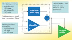
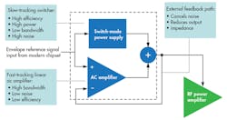
It’s possible to overcome these limitations by adding a high-bandwidth linear (ac) amplifier to the ET IC to create a “hybrid” architecture. This is conceptually similar to multiple loudspeakers in an audio system, in which a “woofer” handles the high-power/low-frequency content, and a smaller “tweeter” provides the high-frequency components.
In hybrid ET architectures, the SMPS handles the dc and low-frequency components of the ET supply waveform, which contain most of the energy consumed by the PA (typically 85% to 95% depending on the waveform statistics). The SMPS can achieve very high energy-conversion efficiency—90% is a good benchmark—and the hybrid architecture doesn’t require a high switching rate.
The ac amplifier then provides the high-frequency components of the ET supply waveform, delivering the high signal bandwidths required and, depending on the details of the ET IC architecture, cleaning up noise generated by the SMPS. The ac amplifier is usually biased in a class AB configuration, which can only deliver theoretical efficiencies of around 40% to 50% for the ac amplifier itself. However, since only a small portion of the energy supplied to the PA is delivered by the ac amplifier (perhaps only 5% to 10%), the effect on the ET IC’s overall energy efficiency isn’t dramatic.
The switcher and ac amplifier can be configured in one of two topologies—either the switcher “leads” the amplifier or the switcher “follows” the amplifier. Both options offer better real-world performance than the standalone fast dc-dc converter, although many detailed tradeoffs still must be made.
When the switcher “follows” the linear amplifier, it senses when the ac amplifier output stage is approaching its output-stage current limit. The switcher then reacts to this current limit by dumping current into the PA supply. This “reactive” architecture introduces a delay between the switcher and amplifier, with the result that as the bandwidth increases, the switcher and linear amplifier increasingly fight each other. This can waste power, leading to an ET IC with a significant fall-off in efficiency at high bandwidth, effectively limiting the useful bandwidth of the solution.
Alternatively, by having the switcher “leading” the ac amplifier (Fig. 2), the ET IC operates in a “proactive” mode—the linear amplifier simply fills in the gaps between the low-frequency tracking provided by the switcher and the high-bandwidth envelope reference signal. In hybrid architectures, the ac amplifier also fulfills an important function by cleaning up any noise introduced by the switcher.
At this point, it’s important for designers to consider exactly which performance metrics they need from an ET modulator and make the necessary architectural and design decisions. For some applications, bandwidth may not be a significant limiting factor, whereas in other scenarios it may be more important to have an ETIC that doesn’t compromise efficiency at high instantaneous channel bandwidths.
For some vendors, it’s also important that a solution can scale beyond today’s 20-MHz requirement for LTE to the 40 MHz needed for carrier aggregation in LTE-Advanced, or the 80- and 160-MHz bandwidths required to support 802.11ac Wi-Fi.
Future Integration Possibilities
One other factor to consider is the potential need for future integration. For designers focused on long-term product roadmaps, having an ET architecture that’s more suitable for integration with a PA will be key to enabling ongoing reductions in size and cost.
For example, integration is less straightforward for hybrid architectures in which the switcher follows the linear amplifier. They require the switcher to be inserted “in the loop” between the ET IC and PA. As a result, it becomes difficult to integrate monolithically with the PA, and adds a noisy SMPS in close proximity to the sensitive RF signals.
Architectures in which the linear amplifier sits after the switcher allow for simpler integration of the ac amplifier and PA at a module or monolithic level. Thus, it’s easier to maintain clear separation of the switcher from these noise-sensitive areas of the design.
Some ET architectures can also be extended to a “distributed” ET solution, where the switch-mode supply is separated out into a different chip altogether. This is particularly useful in MIMO and multi-PA solutions, in which a single ET switcher can provide the low-frequency/high-power components for multiple PAs.
This file type includes high resolution graphics and schematics when applicable.
The ET switcher can be integrated with other similar power-supply circuits into a separate power-management IC. Each PA would be provided with a dedicated local ac amplifier, which may be integrated either at the PCB level, module level, or monolithically on the same die.
The Future of the RF Front End
Given the rise of LTE smartphones and the future requirements of next-generation wireless standards, the RF front end has turned into a huge growth area. In fact, it offers one of the most stimulating and exciting design challenges in IC design today.
To achieve the best performance results with ET, creative and highly skilled analog, RF, and switch-mode IC designers must work together to deliver complex solutions that solve a number of conflicting and challenging design requirements. However, OEMs and modem chipset vendors also need to consider how best to use their resources. Is low-bandwidth LTE performance today more important than the longer-term product roadmap? Can they spare resources to respin their platform firmware and RF architectures each time a new product variant rolls out?
These rather significant questions require serious consideration. Still, regardless of which route OEMs choose to take, the fact remains that ET has undoubtedly become an essential technology for future RF front ends.


