This file type includes high resolution graphics and schematics when applicable.
ADIâs AD9371 wideband transceiver solution boasts two independent transmitter paths and two independent receiver paths, with an RF tuning range from 300 MHz to 6 GHz.
The evolution of transceiver technology permitted the integration of multiple wideband transmitters and receivers on a single chip. The resulting solutions provide a reduction in SWaP (Size, Weight, and Power) without decreasing performance. Such an approach has allowed some transceiver ICs to promise early 5G support.
One attribute that can allow a product to target 5G is wideband operation. For example, the latest addition to ADI's new wideband Radio Verse Family is the AD9371. This wideband transceiver solution boasts two independent transmitter paths and two independent receiver paths, with a RF tuning range from 300 MHz to 6 GHz (see figure).
The AD9371 uses a typical wireless radio transmitter in a direct-conversion, Zero Intermediate Frequency (IF) architecture. Here, input RF signals to the receiver are mixed with LO signals at the same frequency to produce a signal at the baseband (Zero IF receiver). The AD9371 provides all the digital processing, mixed-signal, and RF blocks to implement such a conversion.
Thanks to its programmability, the AD9371 allows the two receivers channels and two transmitter channels to support both Frequency Division Duplex Systems and Time Division Duplex Systems. This function is particularly useful if the IC will be used for test-and-measurement equipment supporting multi-mode testing and multiband applications.
Although the IC’s power consumption depends on the exact configurations, including bandwidth and features enabled, it typically consumes approximately 5W. Specifically, it uses 2W for the two receivers, 2W for the two transmitters, and 0.8W for the observation receiver.
The chip, which is manufactured in 65-micron CMOS, comes in a 12 × 12 mm, 196-ball CSP-BGA package. Because of its reduced component count, it targets applications ranging from light pole installations to office walls, basestations, military satellite communication (satcom) systems, unmanned aerial vehicles (UAVs), and more. In addition, the chip can be used in applications that require low power consumption by 3G/4G micro and macro BTS equipment, both in frequency division duplex (FDD) and time division duplex (TDD) applications.
The 5G Path
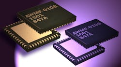
Meanwhile, another transceiver is taking a different path to 5G by operating on the new spectrum bands recently allocated by the Federal Communications Commission (FCC) for development of 5G cellular networks. Specifically, the AWMF-0108 from Anokiwave is targeting 5G communications antenna array applications with a silicon quad-core IC. This Ka-Band transceiver IC covers 27.5 GHz to 30 GHz and supports four radiating elements. The AWMF-0108 is a half-duplex transceiver that enables a single antenna to support both Tx and Rx operation, Tx power telemetry, and fast-beam switching using eight on-chip beam weight storage registers.
As future wireless networks start handling higher frequency bands, the demand for multi-mode/multi-band functionality increases, as well as the demand for supporting multiple standards. Future transceivers are adapting to these demands in the race to provide more support to 5G wireless networks.
This file type includes high resolution graphics and schematics when applicable.


