MIPI D-PHY v1.2 Helps Save Cost, Power in Image-Sensor and Display Apps
The smartphone market has reached an inflection point. It’s considered saturated in developed countries where users can now afford to replace their existing smartphones with new, more sophisticated devices. As a result, minimal smartphone market growth is expected in these countries. To give a boost to their total available market, device manufacturers have begun delivering lower-cost, yet high-quality, smartphones to new users in emerging markets.
Thus, the trend is to replace basic and feature phones with devices that provide high-end smartphone functionality at a lower cost. However, catering to the needs of users in different markets poses unique challenges to manufacturers that provide mobile solutions.
This file type includes high resolution graphics and schematics when applicable.
High-end smartphones and other mobile devices (tablets, phablets) drive technological innovations, but such innovations will need to be delivered in an integrated solution at an attractive price, targeted to new users. Innovations include integration of multiple image sensors that offer superior resolution on the mobile-device display. To support the high throughput required by high-end mobile devices, high-speed interfaces transfer data to and from the embedded storage device, image sensors, and displays to enable image and video capture as well as high-resolution playback.
Advanced multimedia features are driving device manufacturers to integrate innovative peripherals such as multi-megapixel cameras in high-end mobile devices. In turn, integrating these features brings new power, time-to-market, and cost challenges to mobile semiconductor IC designers. While aiming to reduce cost and power consumption, designers must continue to push design innovation boundaries. Therefore, it’s imperative to integrate the latest interface IP that’s optimized for power and helps shrink cost and time-to-market.
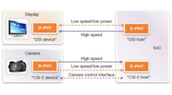
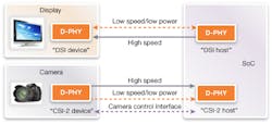
The MIPI Alliance CSI-2 (Camera Serial Interface) and DSI (Display Serial Interface) protocols based on the MIPI D-PHY are widely used in mobile devices. They act as a standard interface between application processors and displays (using DSI) or cameras and image sensors (using CSI-2). MIPI protocols are designed and optimized to service the specific features required for image sensor and display applications while minimizing costs and power consumption. The MIPI D-PHY, the physical layer used for MIPI CSI-2 and DSI applications, connects image sensors and displays to systems-on-a-chip (SoCs) in mobile and embedded applications. The D-PHY provides an economical way of implementing high- and low-speed traffic connecting to the protocol layer via PHY-Protocol Interface (PPI) connectivity (Fig. 1).
The D-PHY is a source synchronous, lane-based, serial physical layer that consists of a single clock lane and one or more data lanes. Since the connection is source-synchronous, the clock is provided from one side of the link (called the master) and isn’t embedded with the data. This configuration simplifies circuit design because complex clock and data recovery (CDR) circuitry isn’t needed at the receiving end. Unlike other SerDes architectures that use data encoding (such as 8b10b that turns each byte of data into a 10-bit symbol), the D-PHY doesn’t require a byte-oriented coding scheme and its data doesn’t carry overhead.
Power Reduction
The D-PHY’s scalability helps save power. It uses a selectable number of data lanes and can shut down unused data lanes. Data lanes are typically used in the unidirectional mode in high-speed transmissions, where a Master D-PHY and Slave D-PHY source and receive the clock, respectively. For example, a DSI Host application implemented on the SoC side employs a Master D-PHY to source the signal to the display on the board, while a CSI-2 Host application uses a Slave D-PHY to receive the signal from the image sensor.
Because the D-PHY isn’t bound to specific rates, it can optimize power consumption based on the traffic generated when sourcing a clock signal that corresponds to the actual required data rate. This flexibility creates a cost-effective solution by removing the need for unnecessary memory buffering and design complexity. In addition, the D-PHY supports high- and low-speed (or low-power) operation. High-speed transmission uses the clock lane, while low-power operation utilizes the self-clocked data to save power, while the clock lane stays idle.
Higher Data Rates
Though the D-PHY specification was originally built to support rates of 500 Mbits/s per lane, in 2009 the high-speed burst mode offered up to 1000 Mbits/s per each lane. With this data-rate increase, the D-PHY specification gained widespread adoption for mobile-camera and display protocols. Users then reached a consensus to push speed to 1.5 Gbits/s maximum, which was implemented in the D-PHY specification v1.1 in 2011.
The recent release of the MIPI Alliance D-PHY v1.2 specification extends the capabilities of D-PHY high-speed burst to 2.5 Gbits/s per lane. Developers of displays and image sensors can now leverage the same design and architecture to support aggregated bandwidth of up to 10 Gbits/s using four data lanes, or 20 Gbits/s using eight data lanes.
The release of the D-PHY v1.2 specification included throughput enhancements, yet the industry must continue to target ways to cut cost and power. The updated specification can be used in two possible ways:
1. Extend the bandwidth to up to 10 Gbits/s using a similar, proven architecture in high-end image sensors or displays. For example, using four lanes of D-PHY v1.1 specification could carry up to 6 Gbits/s, while a similar implementation using the D-PHY v1.2 specification can now carry up to 10 Gbits/s and support 20- to 40-Mpixel image sensors.
2. Carry the same amount of data in fewer data lanes. For instance, an image-sensor design capable of running four lanes at 1.0 Gbits/s, thus providing a throughput of 4 Gbits/s, can now be packed into two lanes operating at 2.0 Gbits/s. This saves silicon area and power consumption, and reduces pin counts.
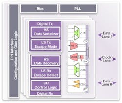
With its mix of features, cost, and power consumption, Synopsys’ IP has enabled many customers to reach production. The DesignWare MIPI D-PHY IP cuts cost and area by half and, according to the company, is the industry’s first D-PHY that complies to the MIPI Alliance D-PHY v1.2 specification, enabling speeds of up to 2.5 Gbits/s per lane (Fig. 2). The DesignWare MIPI D-PHY IP minimizes time-to-market and maximizes ROI with its configurability options and variety of solutions for CSI-2 and DSI applications, reducing the number of SoC designs required to support multiple applications.
This file type includes high resolution graphics and schematics when applicable.
The new DesignWare MIPI D-PHY IP currently comes in 16-nm FinFET processes, and will be available in 28-nm processes in early 2015. Verification IP for MIPI D-PHY v1.2 is also available now.
For more information about Synopsys MIPI IP, visit the company's Website.
Additional Resources


