Synchronous Buck Converter Delivers 12 A With Fast Load Step Response
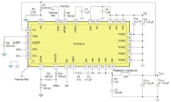
Texas Instruments’ TPS53915 (Fig. 1), can supply up to 12 A output that is adjustable from 0.6 V to 5.5 V. Its input voltage ranges from 1.5 V to 18 V. A 4.5 V to 25 V VDD input powers an internal 5 V LDO that supports internal functions. Other features are auto-skip mode operation, internal soft-start control, and no requirement for compensation. A forced continuous conduction mode helps meet tight voltage regulation accuracy requirements for performance DSPs and FPGAs. A default switching frequency (fSW) pre-set to 400 kHz can be changed to 1 MHz under PMBus control. Available in a 28-pin QFN package, the TPS53915 is specified for operation from –40 °C to 85 °C ambient temperature.
Related Articles
- 15-V, 200-mA Synchronous Buck-Boost DC/DC Converter
- 100-mA Synchronous Buck Converter Features 150 V Input Capability
- 40VIN/OUT, 2A Synchronous Buck-Boost DC/DC Converter
- 30-A, 15-V Synchronous Buck Converter
- 12-V dual-channel synchronous buck converter with integrated FETs
- 10-A Synchronous Buck Converter With Integrated FETs
TPS53915’s D-CAP3 mode control combined with adaptive on-time architecture, results in low-duty-ratio and ultra-fast load-step-response. Adaptive on-time control tracks and controls the preset switching frequency over a wide range of input and output voltage while increasing switching frequency as needed during a load-step transient. This control scheme does not require an external phase-compensation network, which enables a low external component count. Fig. 2 shows a simplified buck converter using the D-CAP3 mode control architecture.
This proprietary mode control architecture includes an internal ripple generation network that enables use of very low-ESR output capacitors, typically ceramic types. The ripple generation network emulates the ripple component of the inductor current information and then combines it with the voltage feedback signal to regulate loop operation. D-CAP3 control architecture does not require an external current sensing network or voltage compensators.
D-CAP3 control without external compensation has a minimum and/or maximum range of the output filter it can support. An output filter used with the TPS53915 is a low-pass, double-pole L-C type. At low frequencies, the output setpoint resistor divider network and the internal gain of the TPS53915 set the overall loop gain. At the output filter frequency, the gain rolls off at a –40 dB per decade and the phase drops rapidly. The internal ripple generation network introduces a high-frequency zero that reduces the gain roll off from –40 dB to –20 dB per decade and increases the phase to 90 degrees, one decade above the zero frequency.
The inductor and capacitor in the output filter must locate the double pole close enough to the high-frequency zero so that the phase boost provided by the high-frequency zero provides adequate phase margin for its stability requirement. After identifying the application requirements, you should design the output inductance so that the inductor peak-to-peak ripple current is approximately between 25% and 35% of the ICC(max) (peak current) in the application.
Sample and Hold
A sample and hold circuit is an advanced control scheme that improves the TPS53915’s output voltage accuracy. This circuit generates a new DC voltage of CSNwhich is the Sampled-and-Held output of the internal ripple synthesizer instead of the voltage produced by RC2 and CC2 (Fig. 2), which previously added the ripple ramp to the VFB signal and generated DC offset and wider DC accuracy. This Sample-and-Hold technique (patent pending) eliminates the DC offset and allows tight output voltage accuracy.
As the output current decreases from heavy load condition, the inductor current also decreases until the rippled valley of the inductor current touches zero level. This level is the boundary between the continuous-conduction and discontinuous-conduction modes. The synchronous MOSFET turns off when it detects this zero inductor current. As the load current decreases further, the converter runs into discontinuous-conduction mode (DCM).
The TPS53915 uses an adaptive zero-crossing circuit to perform optimization of the zero inductor-current detection during skip-mode operation. Adaptive zero-crossing prevents SW-node swing-up caused by too-late detection and minimizes diode conduction period caused by too-early detection. As a result, the IC provides better light-load efficiency.
When the MODE pin (Fig. 1) is tied to the PGOOD pin through a resistor, the IC operates in continuous conduction mode (CCM) during light-load conditions. During CCM, the switching frequency maintains an almost constant level over its entire load range, which is suitable for applications requiring tight control of the switching frequency at the cost of lower efficiency.
A power-good output goes high when the switcher output is within its target. The power-good function is activated after the soft-start operation is complete. If the output voltage becomes within ±8% of its target value, internal comparators detect the power-good state and the power-good signal becomes high after a 1 ms internal delay. If the output voltage goes outside of ±16% of its target value, the power-good signal goes low after a 2-μs internal delay. The open drain power-good output must be pulled-up externally with a resistor to VDD.
Overcurrent Protection
Monitoring inductor current during the OFF state enables cycle-by-cycle overcurrent limiting control. The IC maintains the OFF state during the period when the inductor current is larger than the overcurrent trip level. The TPS53915 supports temperature compensated MOSFET RDS(ON) sensing that provides cost-effective accuracy.
The IC monitors a resistor-divided feedback voltage to detect overvoltage and undervoltage. When the feedback voltage becomes lower than 68% of the target voltage, a UVP (undervoltage protection) comparator output goes high and an internal UVP delay counter begins counting. After 1 ms, the TPS53915 latches OFF both high-side and low-side MOSFETs drivers.
When the feedback voltage becomes higher than 120% of its target voltage, the OVP (overvoltage protection) comparator output goes high and the circuit latches OFF the high-side MOSFET driver and turns on the low-side MOSFET until reaching a negative current limit. Upon reaching the negative current limit, the low-side FET turns off and the high-side MOSFET turns on again for a minimum on-time. The TPS53915 operates in this cycle until the output voltage is pulled down under the UVP threshold voltage for 1 ms. After the 1 ms UVP delay, the high-side FET latches off and low-side FET latches on. The fault is cleared with a reset of VDD or by re-toggling EN pin.
Out-of-bounds (OOB) overvoltage protection protects the output load at a much lower overvoltage threshold of 8% above its target voltage. OOB protection does not trigger an overvoltage fault, so the device is not latched off after an OOB event. OOB protection serves as an early no-fault overvoltage-protection mechanism. During OOB, the IC operates in forced PWM mode only by turning on the low-side MOSFET, which quickly discharges the output capacitor, causing the output voltage to fall quickly towards its setpoint. During the operation, the cycle-by-cycle negative current limit is also activated to ensure the safe operation of internal MOSFETs.
The IC also protects itself against overtemperature by monitoring its internal temperature. If the temperature exceeds the threshold value (typically 140 °C), the TPS53915 shuts off. When the temperature falls approximately 40°C below the threshold value, the IC turns on. Thermal shutdown is a non-latch protection.
The PMBus
The IC’s PMBus interface provides program flexibility, supporting a direct format for write operation. Read operations are supported for both combined format and stop separated format.
The TPS53915 allows up to 16 different chip addresses for PMBus communication, with the first three bits fixed as 001. The address selection process is defined by the resistor divider ratio from VREG pin to ADDR pin, and the address detection circuit starts to work only after the VDD input supply has risen above its UVLO threshold.
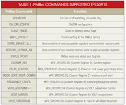
The TPS53915 supports only those PMBus commands listed in Table 1. Not all features of each PMBus command are supported. The CLEAR_FAULTS, STORE_DEFAULT_ALL and RESTORE_DEFAULT_ALL commands have no data bytes. The non-volatile memory (NVM) cells inside the TPS53915 can permanently store some registers.
Plus, the TPS53915 supports FAULT monitoring and reporting through the STATUS_ WORD command.
Also, T.I.’s Fusion Digital Power Designer is a Graphical User Interface (GUI) that can be employed to configure and monitor the TPS53915 design. It uses the PMBus protocol to communicate with the device over a serial bus by way of a TI USB adapter. Tasks performed with the Fusion GUI include:
· Turn on or off the power supply output, either through the hardware control line or the PMBus OPERATION command
· Continuously monitor real-time data, such as VIN, VOUT, IOUT, temperature, and warnings/faults.
· Configure common operating characteristics such as VOUT Margin levels, UVLO thresholds, Soft Start, Power-On Delay, Powergood Delay, Hiccup or Latch off Short-circuit Protection, and switching frequency
· The TPS53915 is also supported by TI’s WEBENCH Design Tool.
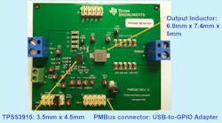
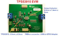
In addition, Fig. 3 shows an evaluation module that supports the design of a TPS53915 power supply.


