Driving And Protecting IGBTs In Inverter Applications
Designing a motor drive or inverter systems using a gate drive optocoupler driving MOSFET buffers helps to maximize IGBT gate drive design scalability from low to high power systems.
Switching using IGBTs is common in motor drive and power inverter applications. The drive electronics need to control current flow ranging from tens of amps to hundreds of amps depending on the size of the motor or power system. Building various drive control cards would be inefficient and wastes design resources. A motor drive system that can be easily scaled to accommodate different size motors while remaining reliable and safe is a much better scenario. We will show how a gate drive optocoupler with MOSFET buffer driving capability, optical isolation, and integrated safety features addresses the needs of motor drive and inverter systems.
Related Articles
- High Speed IGBTs Take on the Super Junction MOSFET
- 600V GenX3 XPT IGBTs Exhibit Improved Operating Characteristics
- Ultra-Fast 1200 V IGBTs Reduce Switching and Conduction Losses
- Shielded Optocouplers Prevent Upset in Off-line Switching Power Supplies
- Optocouplers Support High Power, High Speed Inverters
- Optocouplers Safely Isolate Integrated Power Modules
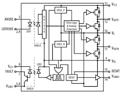
The ACPL-339J is an advanced 1.0A dual-output, easy-to-use, intelligent IGBT gate drive optocoupler interface (Fig. 1).
Uniquely designed to support MOSFET buffers of various current ratings while providing valuable optical isolation in the system, the ACPL-339J makes it easier for system engineers to support different system power ratings using one hardware platform by interchanging the MOSFET buffers and power IGBT/MOSFET switches. This concept maximizes gate drive design scalability for motor control and power conversion applications ranging from low to high power ratings. The ACPL-339J also contains integrated short circuit protection, under voltage lockout (UVLO), “soft” IGBT turn-off, and isolated fault feedback to provide maximum design flexibility and circuit protection.
Scaling Designs
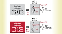
One of the key requirements of a gate drive optocoupler is its ability to provide high peak output current to charge or discharge the gate of the IGBT quickly to prevent switching loss. Avago gate drive optocouplers have output current ratings ranging from 0.4 A up to 5 A which can be used to drive small IGBTs directly. For IGBTs with higher ratings, a discrete PNP/NPN bipolar buffer stage is usually used. By changing the buffer stage to a MOSFET driver, it is possible to maximize gate drive design scalability and power conversion efficiency.
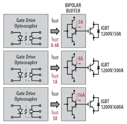
Fig. 2 shows how different bipolar buffers are used to drive different class of IGBTs from 50 A to 600 A. As the size of IGBT gets bigger, higher peak current is required at the gate of the IGBT to turn it on efficiently.
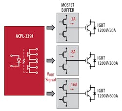
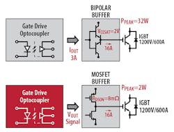
The magnitude of the bipolar’s output current is a factor of its base current, IB and the transistors current gain, β. In another words, gate drivers with different peak output currents and matching bipolar buffers are needed to achieve the peak gate current required by different class of IGBTs. MOSFET buffers, on the other hand, are voltage controlled devices and their current amplifications are independent from the previous gate driver stage. Fig. 3 shows MOSFET buffers with different internal turn-on resistance, RDSON to deliver the peak gate current required by the different classes of IGBTs. Although the ACPL-339J output is specified at 1 A, the switching of the MOSFET buffers will happen as long as the ACPL-339J output voltage crosses the input threshold of the MOSFET buffers.
The ACPL-339J makes it easier to support different system power ratings using one gate drive platform by interchanging the MOSFET buffers and power IGBT/MOSFET switches. All these changes can be made without redesigning the critical circuit isolation and short circuit protection.
Lower Power Losses
A bipolar buffer uses a compounded structure consisting of two or more transistor stages cascaded to achieve high current gain. The drawback is the increase in saturation voltage, VCESAT and the fact that the output is not able to pull to the rail. This results in high power losses when the bipolar buffer delivers high peak output current to the gate of the IGBT. The power lost by the bipolar buffers increase tremendously as higher peak current is needed by the gate of the IGBT. A MOSFET buffer has a “rail-to-rail” output and the internal turn-on resistance, RDSON gets smaller when delivering higher peak current. The MOSFET buffer in Fig. 4 shows significant power reduction when compared to the bipolar buffer delivering the same peak current.
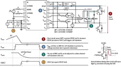
The IGBT’s collector-emitter voltage can be monitored by ACPL-339J DESAT pin during IGBT normal operation. When a short circuit occurs, high current flows through the IGBT and it comes out of saturation, into desat mode. This causes the IGBT’s collector and emitter voltage to increase rapidly from a saturation voltage of 2 V. Once its crosses the ACPL-339J’s threshold of 8 V, a short circuit fault is registered and soft shutdown is triggered. The ACPL-339J’s VGMOS pin will switch on an external transistor to slowly discharge the gate of the IGBT to achieve the soft shut effect. The rate of the soft shutdown can be adjusted by the size of the external transistor and resistor to minimize the overshoot at the IGBT. Lastly, the entire desat operation is completed by reporting the fault through a built-in insulated feedback path to the controller. This short circuit protection process is shown in Fig. 5.
