Integrated Physical Datapath Technology Delivers Predictable QOR, Reduces TTM and Enables Reuse
High-performance communication system-on-chip (SoC) designs targeting smart phones make heavy use of datapath-centric blocks, including adders, shifters, multipliers, memories and highly interconnected blocks such as crossbar switches. The challenge with these complex design blocks is that they have high cell density and connectivity and typically require custom placement and routing in order to achieve predictable quality of results (QoR) and meet tight design schedules. These benefits are generally associated with a standard-cell place-and-route (P&R) flow, and SoC designers would gain from an approach that integrates custom block implementation with a digital P&R flow to leverage the same benefits.
This article introduces integrated physical datapath technology, based on structured placement, optimization and routing that provides such an optimal approach. It also shares Qualcomm’s successful usage of this technology on key design blocks in their 16nm FinFET and 20nm SoC designs to achieve predictable QoR, reduce time to market (TTM) and enable design reuse.
Custom Design Challenges, Move To An ASIC Flow, And Increasing Use Of IP
Datapath optimization techniques have been around since the beginning of general-purpose microprocessor design. The primary objective is to control the physical aspects of the datapath, minimize the distance between the driver and its sinks, and make better use of routing resources. Since then, design complexity and market requirements have changed significantly. The old 8-bit fixed-point microprocessors are now 64-bit processors with floating-point units using 128-bit datapaths. Also, due to shorter schedules, designers have to use regular libraries and ASIC flows. Implementing datapath-centric blocks in an ASIC flow requires tiling or structured placement to adequately support the regularity of datapath cells. This critical characteristic is generally not well supported by standard P&R tools; hence, most datapath designers implement datapath blocks manually using custom approaches. Custom design challenges highlighted in (Fig. 1) have prompted designers to minimize the usage of custom flows and move to standard P&R flows offering an integrated and automated physical datapath capability.
Furthermore, SoC designers are embracing design reuse techniques and integrating intellectual property (IP) blocks to meet the demands of increasing on-chip functionality and shorter design schedules. This trend is highlighted in (Fig. 2). The decision to buy external IP or to develop in-house IP requires careful consideration, taking into account functionality, verification and implementation aspects, project schedules and more. Datapath structure is a key element of IP blocks and can be as critical as the correctness of the logic. If the design team is not familiar with the external IP and its critical blocks (such as the datapath), QoR and project schedules can be impacted. Companies today are developing internal blocks as IP for a variety of reasons: internal IP is company owned and differentiated; it delivers predicable QoR; and it can be used in SoCs targeting different applications at different process nodes.
Successful Deployment Of Integrated Physical Datapath – Qualcomm’s Perspective
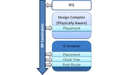
Qualcomm was implementing a high-performance communication SoC with multiple datapath centric blocks. In order to achieve predictable QoR and benefit from integration and automation, the company decided to use the physical datapath capability in IC Compiler to define, analyze and implement datapath and custom blocks in a standard-cell implementation flow. To define custom blocks, Qualcomm specified the relative column and row positions of instances using simple built-in Tcl commands, called relative placement (RP) constraints. The RP constraints were developed at the gate level to preserve datapath elements so that they were not decomposed during optimization ̶ for example, preventing a MUX from being decomposed into NAND and NOR gates. The RP constraints arranged standard cells in row/column structures known as RP groups. RP groups were analyzed in the GUI, refined during placement and optimization, and fully preserved through legalization, clock tree synthesis (CTS), routing and post-route optimization. A primary advantage of the Synopsys physical datapath flow, shown in (Fig. 3), is that RP constraints can be transferred seamlessly between synthesis and P&R.
Qualcomm used the aforementioned physical datapath technology on multiple blocks to meet its QoR objectives, reduce TTM and enable IP reuse. The success of this approach is highlighted through the following two design applications:
- 1024x1024 Crossbar design: For this very routing-intensive block, the main objective was to minimize congestion and achieve the most optimal QoR.
- Full custom flow: Here, the main objective was to develop a semi-custom, reusable flow using standard P&R implementation.
1024x1024 Crossbar Design
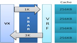
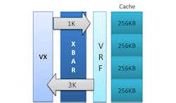
The Crossbar (XBAR) design is the interface between the Vector Execution Unit (VX) and the Vector Register File (VRF), as shown in (Fig. 4). The XBAR data inputs are 32 x 32bit words (1 Kbits) and (1Kbits) bypass signals, and the outputs are 32 x 32bit words (1 Kbits) and another 3K signals forwarding even/odd entries. All these inputs and outputs result in a total of 6K signals crossing the design in the horizontal direction. The physical height of the implementation is restricted by four 256KB cache memories. The process metallization further constrains the implementation to two horizontal and two vertical useful metal routing layers. The XBAR also needs to support instructions such as permutation and broadcasting. In permutation instructions, the order of the 32-bit input words is rearranged and sent to the output. In broadcasting instructions, a 32-bit input word can be sent to all the 32-bit output words.
This functionality makes the internal routing of the XBAR extremely complex, as signals entering the bottom of the design must leave from the top of the design. Careful planning is needed to manage the routing resources efficiently and control the area required to route the signals. If not done properly, longer routes would also require more buffering and consume more power.
Implementation
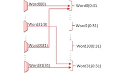
The datapath of the XBAR was implemented using RP with a 32-to-1 bit MUX for each of the 1024 inputs. It was constructed using a combination of 10 four-input MUXes in two levels and a two-input MUX in the final stage. The MUX was constructed in a single row, as shown in (Fig. 5). The preferred implementation would have been to use two rows, but this would have exceeded the height of the four 256KB cache memories and would have required a 2048 standard-cell row height.
With the data flow constructed in a nice pattern, the next challenge was to control the routing. The starting point was defined by the RP bit row. The output location was defined by the output port of the XBAR. The crossbar internal routing is shown in (Fig. 6). A set of pre-routes was generated to control the routing, and buffer areas were provided for longer wires. The final connection (pin-to-pre-route) was done automatically by IC Compiler.
Qualcomm successfully used the Synopsys physical datapath technology to implement a very routing-intensive design. The results included significant improvements in TAT and QoR as shown in (Fig. 7), 6X reduction in runtime, no routing design rule constraints (DRCs) and significant improvements in timing and other key design metrics.
Semi-custom Reusable Flow Using Standard-cell P&R Flow
The Qualcomm SoC includes custom blocks implemented using a custom approach. As discussed previously, this approach is very time consuming and not reusable. The circuit designer has to manually create the schematic, optimize the timing paths, and size the gates to meet timing. Once the circuit designer is done with the schematic, the mask/layout designer has to layout each gate and route each net. In addition, in case any engineering change orders (ECOs) are required, the changes must be done manually, first, in the schematic by the circuit designer, and then implemented by the layout designer.
Semi-Custom Flow
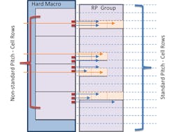
The automation in the P&R tool helped Qualcomm implement the control logic using a semi-custom flow. This control logic is directly connected to the custom blocks. The developers created a semi-custom flow based on the physical datapath technology and pre-routing techniques. RP groups were created and carefully anchored, and group rows were aligned with the hard macros. The hard macros used a non-standard pitch to achieve higher cell density and to target different SoCs. The RP group used a standard pitch that did not align perfectly with the hard macros, created pre-routes, and used IC Compiler to make the final connections, as shown in (Fig. 8).
Using a semi-custom flow reduced a number of costly ECOs and improved runtime. Qualcomm’s SoCs are typically targeted toward multiple applications that require different versions of these semi-custom designs with the same functionality but different memory configurations such as 4KB, 8KB, 16KB, etc. The semi-custom flow enabled these configurations to be easily implemented with Synopsys’ standard-cell P&R solution.
Results
With this flow, the team achieved:
-
Predictable QoR
- The RP groups preserved datapaths through the flow
- Cell placement and routing techniques helped improve QoR
-
Faster TTM
- Integrated physical datapath technology through the P&R flow
- Simple Tcl commands made it easy to use
- Faster closure enabled by fixing violations inside the semi-custom blocks while optimizing the top-level design
- Reduced ECO runtime from days and weeks to hours
-
IP reuse
- Allowed reuse of critical blocks as an internal IP on multiple SoCs and at different technology nodes
Conclusion
The Qualcomm team designing complex communication SoCs has successfully developed an implementation flow based on Synopsys integrated physical datapath technology that delivers predictable QoR, reduces TTM and enables IP reuse. Going forward, Qualcomm plans to extend the use of physical datapath technology into synthesis to help RTL designers better plan their datapaths, and do an early assessment of timing and congestion before handoff to the backend designers.
References:
- Paul Basset, Frank Gover, Tung Pham - Optimizing 1024x1024 Cross Bar Design Employing Relative Placement, Pre-routes and Buffer Pre-placement Flow Austin SNUG 2013
- Paul Basset, Nadeem Eleyan, Frank Gover, Masud Kamal, Ken Lin, Patrick Szabo - Qualcomm DSP Semi-Custom Design Flow: Leveraging Place and Route Tools in Custom Circuit Design https://www.synopsys.com/news/pubs/snug/2012/austin/fc2_paper_eleyan.pdf Austin SNUG 2012
- Jafar Safdar - “The best of both worlds” http://www.eetimes.com/design/eda-design/4216431/The-best-of-both-worlds EE Times May 2011
- Jafar Safdar - Physical Datapath – Improved Productivity for All Designs http://www.synopsys.com/apps/protected/docs/pdfs/iccwp/icc_datapath_wp.pdf Synopsys White Paper 2009
