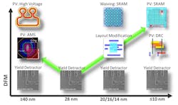
This file type includes high-resolution graphics and schematics when applicable.
In recent years, we’ve seen patterns and pattern matching become a ubiquitous addition to design-verification and design-for-manufacturing (DFM) solutions, and now, process development. By including pattern matching in design verification and DFM, we have both eased and improved how we check, analyze, and score integrated-circuit (IC) designs to achieve better designs faster.
Likewise, fabs and foundries are now adding pattern matching to process development to accelerate process learning, and accelerate and improve the production yield ramp. Interestingly, this synthesis of design rules and patterns isn’t just limited to the most advanced nodes—it’s seen in both established (e.g., 180 nm to 40 nm) and advanced nodes (e.g., 28 nm to 7 nm).
Advanced Node Process and Design-Rule Development
At each new technology node, a foundry or independent device manufacturer (IDM) must first determine what electrical and physical design specifications are needed to be competitive in the marketplace. Then they move on to developing a manufacturing process that achieves these design specifications while delivering stable and high yielding wafers. I’ll refer to this going forward as specification-driven design rules and process development.
The specification-driven approach has been used successfully for many years, and continues to be the primary means of defining and driving development through 5 nm. Tremendous historical knowledge is captured from prior node learning, and extended via shrinks and scaling to the next node as a starting point. This knowledge then becomes specification-driven rules that are used to drive the development of test structures (layouts, sometimes scaled from the prior node) and early signoff reference design-rule-checking (DRC) decks for verification.
Such an approach leverages learning, test cases, and DRC infrastructure from all previous technology nodes to the maximum extent, and enables a foundry or IDM to quickly establish a baseline for the process development of the next node. The design-rule decks and DRC resulting from this process are next used for further process maturation and initial intellectual-property (IP) development, both of which drive further cycles of learning and refinement.
Adding Patterns and Pattern Matching to Accelerate Learning
If traditional approaches to process development are so successful, why have we seen patterns and pattern matching added to this process? One can point to a number of reasons.
First, foundries and IDMs are under ever-increasing pressure to ramp to volume production faster. Second, even in this day of ever-more restrictive design, designers are creative—they still manage to create layouts that a new node process hasn’t seen before. Third, with the industry stuck using 193-nm lithography through at least the initial 7-nm offerings, more and more shapes are in-context, meaning they interact with or affect nearby shapes. These in-context interactions affect lithography, etch, rapid thermal annealing (RTA), 3D topology, etc., in a wide range of known and unknown ways.
Adding Pattern Matching to Advanced Node Process and Design-Rule Development
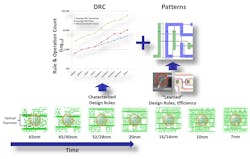
Even very early during process development, and especially once IP development has begun, changes to specification-driven design rules are very expensive—they have an impact across the entire foundry or fab, and even out to IP suppliers and early customers. Supplementing specification-driven process development and design rules, patterns are used as an efficient means of inserting potential design approaches into process development that might ultimately be seen from creative designers, or to efficiently capture a known “yield detractor” pattern from a wide range of sources.
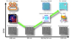
Even if the underlying first principal interactions are poorly understood, using patterns to capture both of these learned “yield detractor” patterns and their counterparts—the “known-good” patterns that must be designed exactly the same way in all instantiations—is a very powerful technique (Fig. 1).
Utilizing patterns to define more localized but problematic areas also makes it easier to capture, communicate, and address new systematic layout issues, while minimizing the impact across the entire ecosystem. The ability to easily and precisely capture and communicate multi-layer layout relationships in a visual pattern enhances the communication of manufacturability knowledge across organizational boundries within a foundry or fab, and between the foundry or fab and the designers.
At the same time, exposure of a broader range of design layouts to a new process is one of the best ways to “harden” the process to achieve yield ramp. However, this exposure can be a challenge with the limited amount of internal IP available to a third-party foundry before the first customer designs are submitted.
To help bridge this gap, pattern-generation tools, like Mentor Graphics' Calibre Pattern Matching and the layout schema generator (LSG) functionality embedded within Calibre LFD, are used to generate arbitrary layout patterns that comply with the targeted design rules. These generated patterns are added to the specification-driven test patterns and other learned patterns from prior nodes to dramatically expand the test-pattern coverage used to mature each new node’s process. This expanded test-pattern coverage is especially valuable in helping prepare the process before customer tapeouts are available.
The Samsung Foundry Closed-Loop DFM Flow (Fig. 2) announced at DAC 2016 incorporates these patterning elements, as well as:
• Profiling incoming designs and analyzing the constituent patterns against what their process has already seen.
• Leveraging silicon test combined with pattern analysis to identify previously unknown yield detractors.
• Using all of this learning to drive more intelligent wafer metrology and manufacturing process optimization for sensitive patterns and design repair.
By incorporating pattern matching in both the design and production environments, Samsung Foundry provides customers with a faster yield ramp. In fact, over 10% yield improvement has been experienced in the initial phase of production. This flow is a great example of how the synthesis of specification-driven design rules with pattern matching can deliver so much more than design rules alone.
Established Node Process and Design-Rule Extension
Business levels at established process nodes are booming. The Internet of Things (IoT) is driving unprecedented production needs at established nodes, and extending the productive life of these fabs. But it also asks much more of the same process than what was demanded when first built. For example, when the 130-nm node process was built at any fab 15+ years ago, the process was first developed and optimized for digital CMOS logic.
To meet the needs of today’s market, we are now trying to build far more complicated IC designs that include new devices and significantly more mixed-signal components, and we’re throwing in some non-Manhattan geometries for microelectromechanical (MEM) or silicon photonics (SiP) devices, etc., for good measure. At the same time, many of the lead process engineers, technology development teams, and design-rule developers who originally put the design rules in place 15+ years ago have moved on to other things (e.g., 7 nm, golf, long walks on the beach), taking their expertise and experience with them.
Synthesis into a Single Flow is Where It Sizzles
Every major EDA supplier has a pattern-matching tool, but that really isn’t enough. In a world where we have synthesis of design rules and patterns, the real leverage is using a tightly integrated set of tools to do something more than what was possible before. You don’t use pattern matching for the sake of pattern matching—you use it to find a specific area of the design to do something else that was once impractical, or not considered.
For example, consider physical verification using a combination of DRC and pattern matching to leverage what each tool does well. DRC is very fast and accurate, and the most effective means of checking and analyzing large areas of a design. Pattern matching is used to describe and find more localized areas with specific polygonal relationships.
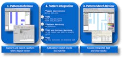
By combining the two, you can create an extended physical-verification process where pattern matching finds and checks potential problem areas in a design, then reports this information along with the pattern-matching output marker showing the associated fix. The DRC tool can then use this information to automatically merge those fixes back into the layout (Fig. 3). Now you have a physical-verification flow that quickly identifies if a design is DRC-clean, and repairs problem areas accurately and precisely.
This sort of layout modification/fixing/retargeting flow is used inside all foundries prior to optical proximity correction (OPC), and is becoming common for fabless companies as well. Moreover, regardless of process node, curved (non-Manhattan) design layouts for mixed-signal, radio-frequency (RF), MEM, and SiP designs are a challenge for traditional verification tools. Combining pattern matching with the expanded verification functionalities of a full-featured DRC tool enables the automated verification of curved structures that historically could only be checked with time-consuming and error-prone manual inspection (Fig. 4).
Conclusion
Whether you’re a fabless semiconductor company or a foundry or IDM, or whether you’re working on your first 7-nm design or at established nodes, the synthesis of specification-driven design rules and pattern matching is changing how you do your job. Single integrated flows combining pattern matching with other verification/analysis tools are enabling foundries and fabless companies to perform physical verification faster and more precisely, fix problematic geometries automatically, accurately verify non-Manhattan layouts, and improve manufacturing ramp up to high yield faster. As the saying goes, “a picture is worth a thousand words.” The same holds true for IC design verification and pattern matching.
