What you’ll learn:
- Cache memory significantly reduces time and power consumption for memory access in systems-on-chip.
- Technologies like AMBA protocols facilitate cache coherence and efficient data management across CPU clusters and IP blocks.
- Implementing cache memory, including L1, L2, and L3 caches, addresses the need for fast, local data storage to accelerate program execution and reduce idle processor time.
- CodaCache enhances data throughput, reduces latency, and improves energy efficiency in SoC designs.
Designers of today’s systems-on-chips (SoCs) are well acquainted with cache in the context of processor cores in central processing units (CPUs). Read or write access to the main external memory can be time-consuming, potentially requiring hundreds of CPU clock cycles while leaving the processor idle. Although the power consumed for an individual memory access is minimal, it quickly builds up when billions of transactions are performed every second.
For context, a single 256-bit-wide data channel running at 1.5 GHz will result in approximately 750 million transactions per second, assuming each transaction is 64 bytes. Multiple data channels will typically be active in parallel, performing off-chip DRAM access.
When a program accesses data from one memory location, it typically requires access to other locations in close proximity. Furthermore, programs usually feature loops and nested loops in which multiple operations are performed on the same pieces of data before the program progresses to its next task.
Understanding Cache Memory in SoCs
Given these challenges of time-consuming memory access, high power usage, and typical data access and processing patterns in programs, a strategic approach becomes essential. The solution is to implement a small, fast cache memory close to the processor.
When the program requests a new piece of data from the main memory, the system automatically retrieves a block of data and loads it into the cache. The processor subsequently performs multiple operations on this locally stored data. Eventually, the new data resulting from these operations is copied back into the main memory.
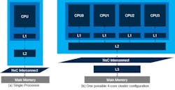
The first level of cache, Level 1 or L1 cache, was followed by adding L2 and L3 caches over time. Each subsequent level is larger and slower than the previous, yet much faster than accessing main memory (Fig. 1).
Another trend is to use clusters of CPUs with varying cache configurations. For instance, in a four-core cluster, it’s typical for each core to have its own L1 cache, pairs of cores to share an L2 cache, and all four cores to share an L3 cache (as shown in Fig. 1b). Alternatively, each core might have dedicated L1 and L2 caches, with only the L3 cache shared among all four cores.
One consideration concerning cache is managing multiple copies of shared data. For example, in the scenario illustrated in Figure 1b, suppose CPU0 retrieves and modifies data from the main memory and then stores the altered version in its L1 cache. Now, imagine that CPU3 wishes to access the same data. Which copy should it use—the original one in main memory or the modified one in CPU0’s L1 cache?
The dilemma leads to the need for cache coherency, meaning that when one copy of data is changed, all other copies must be revised. This may be achieved by updating the data in other caches or by marking the copies in the other caches as invalid.
Cache coherency can be managed in software. However, special hardware is now more commonly used to ensure this happens efficiently and transparently across the caches shown in Figure 1a and within the cluster depicted in Figure 1b.
Modern SoCs, in addition to CPUs, will contain large numbers of intellectual-property (IP) blocks. Some IPs may come equipped with their own caches, which may or may not need to maintain cache coherence with the CPUs.
If coherence with the CPUs isn’t required for any IP blocks, a non-coherent network-on-chip (NoC) interconnect may be employed using the AMBA AXI protocol. Alternatively, if the SoC has multiple CPU clusters that need to maintain inter-cluster coherence, or if IPs with caches need to maintain coherence, then a cache-coherent NoC interconnect can be employed using the AMBA ACE or more modern AMBA CHI protocols.
There’s a third category of coherency called IO coherence, where a device may wish to participate in access to shared memory but doesn’t support full coherency. An example of such an IP would be a GPU accessing shared memory in a way that’s coherent with the rest of the system but can’t directly snoop into the CPU's cache. IO coherent devices rely on the coherent NoC to maintain data consistency on their behalf.
How to Improve SoC Performance with Cache
Other IP functions, such as hardware accelerator IPs, may also benefit from using a cache like the aforementioned CPU examples. These IP-centric caches frequently don’t need to maintain coherency with the CPUs; however, they can be connected using a non-coherent NoC interconnect.
Alternatively, adding a scratchpad memory (SRAM) may benefit some IPs. This high-speed memory is directly connected to the IP to temporarily store small quantities of data for rapid access and retrieval.
Designing a cache or a scratchpad memory is a complex task, even if that cache isn’t required to maintain coherency with other caches. Developers want to spend valuable time architecting the SoC and designing their proprietary IP functions to differentiate their creation from competitive offerings. They often seek to avoid devoting resources to developing a cache.
Implementing CodaCache
One solution is to use CodaCache from Arteris. It’s a configurable, standalone, non-coherent cache IP. Operating at up to 1.2 GHz on SoCs implemented using a 16-nm process technology, CodaCache is interoperable with AMBA AXI and offers up to 8 MB per AXI port. CodaCache provides configurable 1- to 16-way associativity with advanced features like way partitioning, cache flushing, error-correcting-code protection, and support for ISO 26262 functional-safety applications.
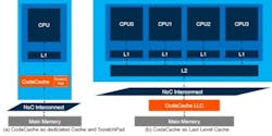
There are many potential implementation scenarios, two of which are illustrated in Figure 2. The first involves adding a dedicated CodaCache to a single IP, providing an IP performance boost (Fig. 2a). The second consists of adding CodaCache as a last-level cache, which boosts SoC performance (Fig. 2b).
CodaCache can also be used in various scenarios, including as a scratchpad memory. Employing a cache in this way offers benefits such as enhanced performance, characterized by increased data throughput and reduced latency. It also promotes energy efficiency by reducing power consumption and heat generation. In addition, it provides design flexibility and scalability, among other benefits.


