What’s the Difference Between Additive and Subtractive Electronics?
This article is part of the TechXchange: PCB Tools and Technology.
Members can download this article in PDF format.
So, you’ve got an idea. It’s brilliant, cutting-edge electronic design. You need to iterate, prototype, and keep your IP safe from prying eyes. When it comes time to bring your project to life, what’s the best way to go about it?
Broadly speaking, there are two processes for manufacturing electronics: subtractive manufacturing and additive manufacturing. Depending on what you’re trying to accomplish, you may need to take advantage of both.
If you’ve been working in electronics for a while, you’re likely familiar with subtractive PCB manufacturing—it’s been the dominant process for 60+ years. But you probably don’t know much about additive electronics manufacturing (also known as printed electronics), or the emerging field of flexible hybrid electronics (FHE).
Subtractive, Additive, and Flexible Hybrid Electronics
Subtractive manufacturing
Subtractive electronics manufacturing is limited to a few core materials options, primarily FR4 or Kapton substrates, with copper to connect the powerful silicon components that have been the driving force behind electronics advancement for the past few decades.
Subtractive manufacturing involves the removal of copper from a substrate via an acid-etching chemical process, leaving behind the traces that form your circuit board, and then soldering on components afterward. It’s an industrial process that uses harsh chemicals and specialized machinery, optimized for mass-production.
When you’re cycling through many prototypes to develop your ideas, subtractive manufacturing can slow your progress with long lead times, supply-chain disruptions, and additional costs associated with minimum order quantity requirements. If you want a solution where you can prototype at your desk, on your own timeline, you may want to consider additive methods instead.
Additive manufacturing
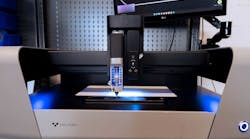
Additive electronics are made by depositing conductive ink onto a substrate to create traces, and then soldering on components. A key advantage of additive electronics manufacturing is fast iteration. The process is ideal when you’re refining your design, with all-in-one PCB printers that can drill, print, solder, and reflow right on your desk. This technology enables rapid iteration and has the benefit of keeping your IP safely in-house.
Another advantage is ease of scaling. If you use direct-ink writing technology during design and iteration, you can make a relatively seamless transition to screen printing for mass-production since both technologies are compatible with the same kinds of inks. In electronics screen printing, conductive ink is forced through a fine mesh screen with a stencil design to create a circuit pattern on your material (the same process used to print graphics onto t-shirts).
With additive electronics manufacturing, you can create rigid PCBs. However, you’re also able to print circuitry onto all kinds of other things, allowing you to create stretchable, flexible, or conformable electronics. There are countless materials options.
Additive methods for manufacturing electronics open up a world of possibilities when it comes to inks, substrates, and technologies—but brace yourself for a learning curve. If you’re working with unconventional materials, it can be difficult to figure out what printing technology to use and/or wrap your head around ink and substrate compatibility. However, the excitement of flexible hybrid electronics (FHE) is leading to a more cohesive value chain and more collaboration in the industry.
Flexible hybrid electronics
FHE is a combination of printed elements (additively manufactured), paired with traditional semiconductor components (subtractively manufactured).
It unites the power of rigid ICs with the plethora of new materials available through additive manufacturing, opening the door to new applications and form factors that have never been possible before. These include medical sensors that interface organically with a patient’s skin, or circuitry printed directly onto the curvature of a rocket.
Note: FHE is not to be confused with flexible PCBs, which are made with Kapton and etched copper, and manufactured with subtractive technologies.
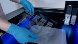
New printing technologies are making it possible to deposit conductive ink onto almost anything, from carbon fiber to glass to biodegradable materials, and even curved surfaces (see figure). A flexible hybrid electronics printer even fits on your workbench, making the technology more accessible than ever.
While FHE is unfamiliar territory for most electronics engineers and designers, it might surprise you to learn that printing electronics isn’t some newfangled process. Additive electronics manufacturing has been around for as long as electronics have existed.
The Evolution of Electronics Manufacturing
In the early 20th century, there was no differentiation between subtractive and additive manufacturing processes. People were just sticking components together with wire, solder, or conductive tape, hoping to make an electronic device—and sometimes burning their house down in the process. Of course, there was nothing that resembled the modern PCB, but early innovators were laying the groundwork that would lead to today’s high-tech electronics.
During World War II, the U.S. and Great Britain started manufacturing fuses for missiles that were built using additive technology, which leveraged a high-heat manufacturing process. Resistors, dielectrics, and conductor paste were screen-printed onto a ceramic board, placed in a kiln at 850°C, and the result was a hybrid microcircuit that looked sharp and refined.
In 1948, the National Standard Bureau held a symposium where they discussed 26 different ways to make electronic circuits, distinguishing the additive and subtractive methods for the first time.
Ten years later, the first integrated circuit (IC) was being developed in Silicon Valley. After a few years of development, the first commercial IC was released in 1964. ICs are heat-sensitive, so subtractive manufacturing was the only compatible technology for incorporating ICs into circuit boards.
Throughout the next few decades of fast-paced innovation, electronics got smaller, more powerful, and more compact. Computers shrunk from room-sized to phone-sized, and the number of ICs on a circuit board doubled with each passing year (today’s ICs have billions of transistors).
Additive electronics manufacturing continued to develop at a slower pace, making progress in a few niche markets—solar panels, blood glucose strips, and Duracell’s printed battery tester—but no one figured out how to incorporate ICs using additive methods.
The turn of the century marked a new era for additive electronics. In 2002, the Defense Advanced Research Projects Agency (DARPA) invested heavily in additive-manufacturing projects as part of its initiative to create breakthrough technologies and capabilities for national defense. Their goal was to find a way to print everything on anything.
Thanks to substantial financial investment, researchers were able to create technologies—direct-write and inkjet printing — that could print conductors, resistors, and insulators. Advances in materials science led to the development of biosensitive inks, thermoelectric inks, electroluminescent inks, stretchable materials, and more.
After all of this progress, the National Research Council identified a need to build an industry around additive electronics manufacturing to foster collaboration, build standards, build stable supply chains, and find ways to incorporate rigid silicon ICs into flexible materials. This led to the new era of flexible hybrid electronics.
The Future of Electronics
While the history of these two methods has led us to where they are today—subtractive is an established manufacturing process for rigid PCBs, and additive electronics manufacturing is just beginning to tap into its true potential — the future of electronics has a place for both. Flexible hybrid electronics is leveraging the best of both worlds, bridging the gap between what we can do and what we wish we could do with electronics.
Read more articles in the TechXchange: PCB Tools and Technology.

