Top 5 Challenges in PCB Assembly
Members can download this article in PDF format.
What you'll learn:
- What's driving the PCB miniaturization trend?
- Main challenges involved in PCB manufacturing and assembly.
What are the main strategies to overcome these challenges? Check out Part 2.
The world of electronics is undergoing a transformational shift driven by the relentless push for miniaturization. As the demand for smaller, more powerful, and feature-rich devices surges, printed circuit boards (PCBs) continue to evolve dramatically in terms of miniaturization to enable such high-density integration.
However, with miniaturization comes unique design and manufacturing challenges that require creative solutions. This article examines the miniaturization trends of PCBs and the top five challenges introduced by miniaturization in PCB assembly.
The Rising Prominence of Miniaturization
The popularity of mobile devices, wearables, the Internet of Things (IoT), and other space-constrained electronics has fueled the movement toward PCB miniaturization. Consider how modern smartphones pack an astounding amount of functionality into a slim and compact package by leveraging advanced PCBs.
Similarly, wearable products like smartwatches must be designed around highly miniaturized PCBs to be convenient and ergonomic. In addition, applications such as medical devices, aerospace avionics, and automotive electronics are driving the need for smaller, lighter, and more power-efficient PCBs.
Drivers and Benefits of Miniaturization in PCBs
Several factors are catalyzing the push for miniaturization in printed circuit boards:
Improved Portability
Smaller and thinner electronics are more accessible to carry around. With the rising popularity of mobile and handheld electronics, having a small and lightweight product is no longer a luxury, but a fundamental need. Bulky electronics are inconvenient to carry around and use on the go. Miniature PCBs help create slimmer and more portable devices.
Integrated Functionality
More components can be integrated into the same footprint area. Greater computing power and functionality are being packed into smaller products nowadays. For instance, a smartwatch today can have cellular connectivity, health monitoring, GPS tracking, and more. Miniaturization makes it possible to fit more components and capabilities into compact devices.
Enhanced Efficiency
Shorter trace lengths in high-density PCBs enable better high-speed signal integrity and data-transmission rates with lower losses. Thus, miniaturization boosts the overall efficiency and performance.
Reduced Power Consumption
Compact designs reduce the overall power transition length, so there’s less energy loss. Besides, compact designs dissipate less heat and require lower power.
Higher PCB densities enable components to be packed more tightly, reducing the overall dimensions. This lowers materials costs since fewer materials are used. Shipping and inventory storage costs are lowered as well due to decreased size.
Product Differentiation
A smaller, more elegant product garners greater consumer appeal and could be a competitive differentiator in the marketplace. Miniaturized designs can also enable differentiated form factors.
Top 5 Challenges in Assembling Miniaturized PCBs
While miniaturized PCBs provide tremendous benefits, effectively manufacturing them poses significant obstacles that need creative solutions. The five most pressing problems are:
1. Challenges in PCB Design
Signal integrity and thermal management are two major issues when dealing with PCB designs.
Maintaining signal integrity is already challenging on standard PCBs. But it becomes even more daunting with miniaturized high-density PCB layouts. The tighter spacing between traces increases parasitic capacitive coupling and trace crosstalk, which can distort signals, especially at higher speeds. Further, impedance mismatches at connections and shorter components lead to increased reflections. This exacerbates issues like ringing and electromagnetic interference (EMI).
Another miniaturization effect is an increase in dielectric constant and loss tangents when distances shrink below 100 μm. This degrades signal fidelity. High-frequency AC signals above 10 kHz are particularly prone to integrity issues. Signal waveforms must retain their intended rise time, amplitude, shape, and timing for proper functionality.
However, even minute signal degradations can disrupt digital logic, serial protocols, clock or data recovery, and analog performance, potentially leading to data loss or corruption. Matching trace impedances, adding ground planes, choosing suitable dielectrics, impedance-controlled routing, and termination resistors help maintain signal integrity. These measures require elaborate modeling, simulation, and analysis, creating cost and effort challenges.
Efficient thermal management is needed to address higher component densities in miniaturized PCBs. Otherwise, excessive heat can build up within such a constrained space. Managing this heat during operation is highly challenging, though.
First, the compact footprint leaves little exposed surface area for heat dissipation through conduction or convection. Miniaturized components packed closely together generate localized hot spots. Second, many ingredients like semiconductors, high-power ICs, and RF chips are inherently heat-sensitive and prone to thermal failures. Their reliability degrades rapidly, with temperatures exceeding threshold levels.
Without effective thermal-management strategies like heatsinks, vias, or fans, the components can undergo accelerated aging, perform erratically, or fail permanently due to overheating. However, it’s difficult to implement traditional cooling solutions given the size and form-factor limitations.
Advanced thermal simulation of the electrical, mechanical, and thermal characteristics combined with strategic cooling techniques is essential during the design process. Thermal-aware component placement and airflow optimization make it possible to manage heat dissipation from dense miniaturized PCBs.
2. Challenges in PCB Bare-Board Production
PCBs are produced with smaller and smaller drills, copper trace width, and space. Also, complex stackups and high layers—up to 100 layers—are designed and produced to address the demands of small size and high density.
Due to limited circuit board space, designers can only reduce line width and line spacing, reduce the diameter of drilling holes, or increase the number of layers. In this case, buried and blind via PCBs and high-density interconnect (HDI) circuit boards are gradually applied to such small-sized but multifunctional electronic devices.
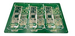
In such printed circuit boards, with 3 mils or less trace width, plating through-hole (PTH) drills are as small as 6 mils, and laser drills as small as 4 mils (Fig. 1). Even blind and buried vias, stacked and staggered vias, and any layer interconnect structure are used.
These bring many challenges and difficulties to circuit-board production in drilling, etching, copper plating, and lamination. So extremely advanced equipment and very skilled CAM engineers and production workers are needed.
3. Challenges in PCB Assembly
Precise component placement and solder joint reliability are two of the challenges companies must address when assembling circuit boards.
Precise component placement is needed because densely packed PCBs have become extremely difficult to design due to ever-shrinking component packages and pad geometries. Standard pick-and-place machines require more precision to position and align miniature components without errors.
Minor placement inaccuracies of even 50 to 100 µm can disrupt the acceptable tolerances and cause significant issues like electrical short circuits, impaired connectivity, signal loss, and reduced reliability. Yet, many miniature components like 01005-size resistors and capacitors can measure just 0.4 × 0.2 mm. Such details demand ultra-precise placement accuracy.
What’s perplexing is that while component sizes continue to decrease, PCB densities are increasing even faster. Thus, the machines need to place more components in less space at higher speeds, stretching their limits. The margin for error is almost negligible.
Therefore, advanced placement systems with high-precision pneumatic nozzles, servo-motor-driven mechanisms, machine learning, and microscopic optics for pattern recognition are essential to achieve reliable miniaturized component placement. However, these solutions also raise the costs and slow the assembly process. It’s a difficult tradeoff.
Solder joint reliability is important as shrinking component sizes and higher densities make these joints increasingly fragile and prone to failure in miniaturized PCB assemblies. Factors like coefficient of thermal expansion (CTE) mismatches, mechanical shocks, vibrations, and flexing introduce strains on delicate solder joints. Flaws like cracks, voids, and cold solder joints commonly arise, weakening the interconnects mechanically and electrically.
Also, during thermal excursions or temperature cycling, these defects can progress quickly into catastrophic solder failures, opening up electrical connections and disrupting functionality.
The root causes are more complex to diagnose and correct on densely packed PCBs. Further, smaller joints have a lower melting point, making them more susceptible to hot spots. Traditional soldering methods must be adapted to achieve robust and reliable solder bonds with miniaturized components.
Solder alloys with blending additives help create more flexible joints. Similarly, advanced solder masks limit bridging risks. In addition, spot soldering and laser soldering allow for localized heating. Overall, enhancing solder joint reliability requires significant process changes.
4. Unremitting Pursuit of Advanced PCB Materials and Smaller Components
Advanced PCB base laminates are needed because smaller circuit boards require improved electrical and mechanical processing performance, high TG, high frequency, high speed, and other high-tech materials that are widely used. For example, reinforced FR4 material can reach a Tg of 200, while PTFE material can reach a Tg of 350.
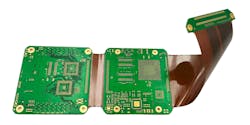
Ceramic materials are also used to meet the high-frequency or microwave requirements of electronic products. Flexible and rigid-flexible circuit boards employ polyimide materials to meet the requirements of lightweight and bendable products (Fig. 2). Products with high thermal conductivity within small sizes will often turn to alumina ceramic materials.
Smaller components are needed because numerous functions and computing capabilities must be implemented on a very small-sized circuit board, and that means more electronic components. However, the size of the circuit board is fixed, so only smaller components can be selected. For example, most passive components are 0201 or the smaller 01005. And the main chips come in space-saving packages, such as STQFP, VQFP, TQFN, VQFN, BGA, and UBGA.
The requirement for miniaturization of electronic components brings great challenges to the design and manufacturing of electronic components. It also increases the difficulty of PCB assembly.
5. Rework and Repair Difficulties
Once assembled, carrying out any necessary rework or repairing the miniaturized PCB becomes challenging. The components are densely packed together with little space between them, leaving little room for error. A minor slip or overheating during manual rework can permanently damage adjacent components or traces.
Furthermore, the integrated nature of assemblies on multilayer boards makes access to repair points difficult. Reworking solder connections increases the risk of thermal damage to surrounding components. Using adhesives or underfill material to separate components makes removal and replacement time-consuming. It’s also more difficult to realign components and secure new mechanical joints.
When attempting rework or repairs on densely packed miniaturized assemblies, extreme caution must be taken to avoid making matters worse and deteriorating workmanship quality. The costs of scrapping and replacing faulty PCBs are also higher. As a result, quality control prior to repair is critical.
In Part 2, we look at practical strategies to address PCB miniaturization challenges.
Read more articles in the TechXchange: PCB Tools and Technology.


