GaN Transistors – Drive Control, Thermal Management, and Isolation
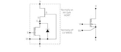
This year, several companies are expected to bring 600/650 V Gallium Nitride (GaN) power transistors to market. Almost all will be normally-on (depletion mode) transistors connected in a cascode configuration with a normally-off MOSFET. This hybrid arrangement, shown in Fig. 1, allows the two devices to provide a convenient, easy-to-drive circuit that has familiar characteristics combined with very special advantages.
The device combination, when carefully designed, will provide the normal MOSFET positive threshold voltage and an enhancement of the already exceptional Figure of Merit (FOM) of the high voltage GaN transistor.
Five companies have shown essentially identical schematics. The very simple circuit shown in Fig. 1 suggests that the driver issues have been clearly and easily solved. There are, however, significant thermal and transient voltage issues to be considered. Any attempt to construct this circuit, without carefully considering these issues, will detract from the realizable performance. The overall performance could even be well short of what an individual GaN transistor is capable.
The key elements for success involve the necessity to:
- Minimize series inductance and resistance
- Minimize thermal resistance
- Provide separate Kelvin connection(s)
- Allow for MOSFET clamping and avalanche control
- Allow for GaN device slew rate control
- Provide sufficient local thermal mass to absorb the transient switching power peak
It is instructive to view the combined device structure as a very high power microwave integrated hybrid device. The GaN transistor will typically provide <20 nS switching time and more than 30 A switching capability. Any significant series inductance at the MOSFET source (S) or at the common node (Cn) will produce unwanted L di/dt transients that can be as large as the threshold voltage of devices – typically plus 2 V for the MOSFET and minus 3 V for a GaN HEMT (High Electron Mobility Transistor) or minus 7 V for a GaN MISFET (Metal-Insulator-Semiconductor-Field Effect Transistor). Additionally, series resistance in the source connection results in debiasing, which produces an apparent increase of the on-resistance. It is therefore vital that short interconnect methods are used and a multiplicity of parallel connections.
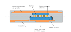
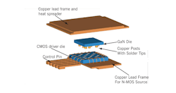
The thermal issues arise because the physical arrangement required to bring the inductance to the minimum results in the two transistors being in very close proximity. GaN transistors that can switch 24 A (1200 V) and 47 A (650 V) have die sizes as small as 2 x 2 mm. The graph shown in Fig. 2 shows the thermal resistance of various GaN transistors. These particular devices are GaN on SiC (Silicon Carbide) transistors that have been optimized for thermal performance by thinning the SiC base wafer down to 100 microns. While this helps considerably, a small square GaN device, sized 2 x 2 mm, (4 mm2) still has a thermal resistance of almost 2°C/W. The GaN 2 x 2 mm, 650 V transistor has an on-resistance of 80 mΩ. The transistor’s ohmic power dissipation would be 32 W if the device were required to sink 20 A. The combination of the device, package and heat sink thermal resistance could exceed, in total 5 °C/W so the temperature increase from the GaN device dissipation alone can exceed 150 °C. The additional dissipation of the MOSFET, assuming a 20 mΩ device is used, would be 8 W. With the total structure dissipating 40 W, the temperature within the package could exceed the safe operating limits – typically 175 °C – of the MOSFET. It is therefore vital to use 2D heat removal, so that the GaN device heat dissipation is channeled out of the package separately from that of the MOSFET. The structure shown in Fig. 3 achieves this result.
Direct Interconnect
This arrangement allows for short copper posts to be used for a adirect interconnect between the large N-channel MOSFET of the driver die and the GaN HEMT die. This structure essentially eliminates intrinsic package problems related to series inductance and resistance.
The 2 x 2 mm GaN device has 12 short copper posts for its source electrodes, and these provide a very low inductance interconnection for the common node. However, because the GaN die is very thin, more than 90% of the heat flow is through the SiC substrate. This allows the MOSFET on the CMOS die to operate within its temperature range.
The lower part of the PQFN lead-frame carries the CMOS die, including the large N-channel MOSFET. Conventional GaN cascode designs use off-the-shelf vertical MOSFET power devices. That approach misses the opportunity to provide a more sophisticated driver because complex integrated structures are not available in the vertical format.
The driver shown in Fig. 3 uses a lateral MOSFET. The large N-channel device is made using a standard CMOS process. As a result, it is possible to add complex control and reporting circuitry that can drive and also protect the GaN transistor. The priority however, is to eliminate the effect of noise that could trigger unwanted switching.
When the simple single N-channel driver shown in Fig. 1 is used, it is vital to provide a “Kelvin Source-Sense” or Kelvin connection (SS). This allows an external driver device to cleanly drive the intrinsic source free of the inductive L di/dt noise generated by the high current fluctuations of the source lead (S). The alternative design approach shown in Fig. 3 and in plan view in Fig. 4 shows an integrated design where a sophisticated CMOS control circuit is monolithically integrated with the N-channel MOSFET switch.
The input circuitry of the CMOS control circuit can include Schmitt trigger differential circuitry and data storage D-type latches. The CMOS die enables the implementation of sophisticiated input circuitry on chip — in fact a complete differential data receiver can be integrated with the MOSFET that directly drives the high voltage GaN transistor, as shown in Fig. 5.
Latching Function
This particular implementation - unique for a power device - provides a latching function and an internal power source that allows the output, M, to remain unchanged in the presence of unbalanced (non-differential) drive signals. In addition, the pre-driver output (M) needs to be kept low until the power source circuit is able to provide sufficient energy for the pre-driver to properly control the driver rise and fall times and enable its clamp action. Non-differential inputs, ll and 00, produce no change in the condition of the large N-channel MOSFET- the device remains either ‘on’ or ‘off’. By cycling the driver IC inputs between ll and 00. the careless pulse transformers provide a narrow pulse that can be rectified to produce the supply voltage needed by the low power control circuit to maintain its status. The majority of the power for the control circuit can only be drawn from the common node (Cn). This source is needed because the N-channel MOSFET has to provide an on-resistance as low as 10 to 15 mΩ and so it has a large gate capacitance with a significant charge requirement .
Therefore, to switch the large MOSFET rapidly on and off, signficant current will be drawn from the VCC supply. The pulse transformers are able to provide the control signal, some modest energy transfer, and of course, isolation. Since the transformer energy transfer is limited, the additional power drawn from the common mode is an important contributor. To achieve safe operation at start-up and power down, the pre-driver output (M) needs to be held low under all power transition and input data conditions.
The isolation method shown uses a coreless transformer, which is superior to conventional optocouplers in terms of jitter, aging and delay. Uneven aging allowances are needed when optocouplers are used, and this results in unwanted switching inefficiencies. It has been reported that some optocouplers have 500nS delay times and 100nS timing mismatch. The internal power is also generated via a coreless transformer. When the Vcc is established, an enable signal L is generated to allow the controllling latch and pre-driver to accept data and provide the drive signal M.
The MOSFET Choice
The CMOS integrated circuit shown in Fig. 5, uses a standard NMOS output structure directly connected to the discrete power GaN transistor. It has been shown that a standard CMOS process can readily provide a large area NMOS device with performance equivalent to discrete, vertically integrated structured low voltage power transistors. This ideal structure is achieved through the use of custom layouts made within the design rules of open GaN and open CMOS foundary suppliers.
The key performance parameters of low voltage power transistors have been examined by the CPES[1] and are shown in Fig. 6.
The Great Wall devices shown are lateral structures. In particular, the Great Wall devices are made using a conventional CMOS process. As the chart shows; providing the voltage requirement is limited to 15 volts and below – a conventional CMOS process provides performance more than adequate for the task.
The critical problem of breakdown voltage brings inductance control and the MOSFET device slew rate control into clear focus. Any significant inductance between the MOSFET drain and the GaN device source will produce an overvoltage condition after turn-off. Circuitry provided on the CMOS chip provides full protection for the MOSFET structure. The clamping/power charging circuit shown in Fig. 5provides some measure of control. However, the NMOS device must also include a local integrated clamp on each of the 12 separate drivers to provide full MOSFET structure protection.
Another concern is the control of the EMC/EMI issues resulting from the dv/dt behavior at the drain of the GaN device. It cannot be assumed that the slew rate control provided by the MOSFET control chip can alone optimize the tradeoff between EMC/EMI issues and speed requirements [2]. Because the GaN HEMT drain/source capacitance does not appreciably change over even a 1000 V transition, this capacitance can provide the basis of a well-defined Miller feedback to the gate of the MOSFET, via its gate/drain capacitance. The drive level and the control circuit’s output resistance driving the MOSFET can be tailored to produce the best tradeoff between EMC/EMI issues and the MOSFET’s switching speed.
Overall Performance
Initial power switch evaluations are usually based upon the inverse FOM – QG × RDS(ON) as shown inFig. 6. Device designers would regard this traditional FOM as simplistic since it only peripherally relates to current limits, thermal factors, and ease of use. But because FOM is a familiar concept, it is still useful to compare GaN transistors and the proposed cascode MOS/GaN hybrid structures on an FOM chart.
Because the performance of a MOS/SiC cascode structure has already been reported [3] it is possible to make this comparison, shown in Fig. 7. This chart also shows a range of FOM performances for MOSFETs, SJ MOSFETs, SiC and GaN devices. Lateral GaN power transistors have achieved between 50 V and 75 V per micron of gate/drain spacing. It is expected that GaN transistors will achieve 100 V per micron in the near term. The blue line is drawn at 66 V per micron. This FOM line suggests that GaN transistors will typically provide an order of magnitude performance advantage over all MOSFET types.
Achieving Desired Performance
The intense interest in GaN transistors has been triggered by the projected performance shown. However, the ease of use issues are significant, the best-performing SiC and GaN transistors are depletion (normally-on) types. To achieve normally-off (enhancement) operation involves degrading the device performance. The cascode approach is therefore a valuable method of providing the required normally-off behavior without compromising performance. The technique is applicable to both SiC and GaN suppliers. The smaller gate voltage swing required by GaN HEMT devices (5 V compared to 15 to 30 V required by some SiC devices), allows standard CMOS processes to be used for the GaN driver circuitry. This is a very significant advantage.
In addition, EPC (Efficient Power Conversion Corporation) using GaN technology has been able to demonstrate highly competitive normally-off low voltage power transistors.
The chart shown in Fig. 8[4] compares state of the art 20 to 40 V Si MOSFET with the 40 V EPC GaN devices. This comparison suggests that it is possible to consider that a monolithic cascode using an integrated low voltage GaN driver device would offer an exceptional performance. It would also be relatively easy to drive with a small CMOS integrated circuit.
The concept would gain truly compelling interest if the normally-off GaN devices could reach toward the performance shown in Fig. 4 by the normally-on RF GaN transistor. Clearly, future three or four terminal GaN devices will probably be monolithically integrated cascode structures (i.e. tetrode) that provide very low input and Miller capacitances.
Future GaN
Five GaN suppliers have announced their intention to introduce cascode structures. The best and most successful of these will include:
- Stacked devices to remove the area penalty
- Stacked devices to reduce inductance
- 2D heat extraction
- Slew rate control
- Enhanced noise immunity
- A FOM 10 to 50 x better than MOSFETs
- Galvanic isolation
- Self-power capability
Therefore, the successful introduction of high-voltage, very high performance GaN depletion transistors depends upon the new cascode-based, hybrid integrated subsystems being easy to use, while also providing system size, cost, and reliability advantages in many applications.
References:
[1] “Technology Roadmap for High Frequency Integrated DC-DC Converter” IPEM C 2009 .
[2] “Controlable dv/dt Behaviour of SiC MOSFET / JFET Cascode”, APEC 2010
[3] Press Release “AOS and SemiSouth demo 1200V Si / SiC stack-cascode MOSFETs” 18 January 2012.
[4] “Simulation and characterization of GaN HEMT in high-frequency switched-mode power converters” Control and Modeling for Power Electronics (COMPEL), 2012 IEEE 13th Workshop.


