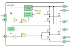
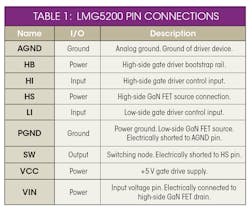
Texas Instruments has packed two GaN FETs and a high-frequency gate driver into a half-bridge configuration that produces an 80 V, 10 A, . The LMG5200 power stage (Fig. 1) features advanced multichip packaging technology and is optimized to support power conversion topologies operating at frequencies up to 5 MHz. LMG5200 inputs are TTL-compatible, and can withstand up to 14 V regardless of VCC. Table 1 describes the LMG5200 pin connections.
The LMG5200 is a complete, reliable power stage, consisting of a performance optimized driver and power GaN FET. All devices are mounted on a completely bond-wire-free package platform with minimized package parasitic elements. Special considerations during package design ensure that the common source inductance, gate loop inductance and power loop inductance are significantly reduced.
This half-bridge GaN power stage integrates two, 18 mΩ GaN FETs with high-side and low-side gate drivers. Including the gate driver in the module improves power-stage efficiency by reducing parasitic inductances in the critical gate-drive loop. Also, propagation delays between the high-side and low-side gate drivers are matched to enable very tight control of dead time. To maintain high efficiency, controlling dead time is critical in GaN-based applications. You can independently control HI and LI inputs to minimize the third quadrant conduction of the low-side FET for hard switched buck converters. A very small propagation mismatch between the HI and LI to the drivers for both the falling and rising thresholds allows for dead times in the range of 10 ns. Co-packaging the GaN FET half-bridge with the gate driver minimizes the common source inductance that impacts hard switched topologies.
This file type includes high resolution graphics and schematics when applicable.
A bootstrap circuit with clamp prevents the high-side gate drive from exceeding the GaN FETs maximum gate-to-source voltage (VGS) without any additional external circuitry. The gate driver has an undervoltage lockout (UVLO) on the VCC and bootstrap (HB-HS) rails. When the voltage is below the UVLO threshold voltage, the device ignores both the HI and LI signals to prevent the GaN FETs from being partially turned on. Below UVLO, if there is sufficient voltage (VCC > 2.5 V), the driver actively pulls the high-side and low-side gate driver output low. The UVLO threshold hysteresis of 200 mV prevents chattering and unwanted turn-on due to voltage spikes.
To simplify manufacturing, the LMG5200’s 6 mm by 8 mm QFN package requires no underfill, sometimes used to meet creepage breakdown requirments. Plus, its reduced footprint increases adoption of GaN power designs in a broad range of applications, from new high-frequency wireless charging to 48 V telecom and industrial designs.
Due to parasitics that can occur during packaging and design layout, GaN-based power designs have had uncertainties associated with their driver circuits. Therefore, designers who use high switching frequency GaN FETs must exercise care with board layout to avoid ringing and EMI. Proper layout of external components used with the LMG5200 is critical to achieving the desired performance. Also, layout of capacitors to provide high frequency decoupling for the gate driver and bootstrap input caps are critical to ensure that there is no loss of gate drive during high voltage switching and current commutation.
To prevent catastrophic failures due to overheating, it is critical that the p.c. board exhibits low thermal resistance with the LMG5200 at the ambient temperature under worst case operating conditions. By following the guidelines for a multilayer board design (http://www.ti.com/lit/an/snva729/snva729) you will obtain the maximum benefit of an integrated gate driver and GaN FET half-bridge module thermally and electrically.
To maximize the efficiency benefits of fast switching, it is extremely important to optimize the board layout for minimum power loop impedance. When using a board with more than two layers you can minimize power loop parasitic impedance by having the return path to the input capacitor (between VIN and PGND) small and directly underneath the first layer. Loop inductance is reduced due to inductance cancellation as the return current is directly underneath and flowing in the opposite direction. It is also critical that the VCC capacitors and the bootstrap capacitors are as close to the device as possible and on the first layer. The AGND connection of the LMG5200 should NOT be directly connected to PGND so that PGND noise does not directly shift AGND and cause spurious switching events due to noise injected in HI and LI signals. Use appropriate spacing in the layout to reduce creepage and maintain clearance requirements in accordance with the application pollution level.
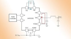
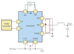
Fig. 2 identifies the impact of board level parasitics on the performance of LMG5200’s key loops. High power loop inductance (shown in red) causes significant overshoot on the switch node. The overshoot causes a loss of efficiency due to increased switching losses. To minimize this loop inductance, it is critical to use layout techniques that effectively eliminate the parasitic loop inductance.
The addition of parasitic switch node capacitance is also a switching loss mechanism as the parasitic capacitor is charged and discharged to the switch node voltage with each switching cycle. Minimize the switch-node capacitance by reducing the overlap between the switch-node plane and the ground and VIN planes. To minimize the added switch node capacitance, it is recommended that there be a cutout for the switch node in the metal 2 plane and possibly the subsequent layers as well. In addition, sensitive control and analog signals should be kept away from the SW pin and the switch-node net to minimize coupling and interference. Locate the power inductor as close to the IC as possible to minimize the area of the switch-node, reducing parasitic capacitance and EMI.
To eliminate spurious loss of input power, minimize the parasitic inductance from the input decoupling capacitors to VCC and AGND. Similarly, to prevent power loss in the high-side driver and cause undervoltage lockout, minimize the added inductance between the bootstrap capacitor and HB-HS by choosing an appropriate capacitor and suggested layout techniques.
This file type includes high resolution graphics and schematics when applicable.
Proper supply bypass of the low-side and high-side drivers is essential in providing stable switching performance without malfunction. Using 0402 sized capacitors, placed immediately adjacent to the IC on the top layer minimizes that the trace inductance for the bootstrap capacitor to HS-HB.
Choose a 0402 capacitor for VCC decoupling to minimize the trace inductance from the capacitor to the VCC, AGND pins. Excessive inductance in these loops can cause a loss of gate drive to the high-side and low-side, which will hurt efficiency and circuit performance. If the inductance is high then a spurious loss of the drive signal below the undervoltage lockout threshold will cause the device to turn off the gate supply completely to prevent damage to the GaN FETs.
In addition to obtaining the LMG5200 evaluation module (EVM), designers can get started faster using PSpice


