Unique Driver Architecture Enhances GaN-Based Isolated Power-Supply Designs
GaN (gallium nitride) E-HEMTs (High Electron Mobility Transistors) have altered the dynamics of power electronics in consumer electronics, datacenters, industrial motors, appliances, and transportation. In the past, the transistor (formerly the Superjunction MOSFET) was the limiting factor in most switching power supplies. For years, 100 kHz-300 kHz was state-of-the-art.
Over the last 10 years or so, the only improvements have been confined to efficiency as MOSFETs have become incrementally better from one generation to the next. With the advent of GaN transistors that look and act like much faster Superjunction MOSFETs, suddenly magnetics, layout techniques, and performance drivers have leapt into the limelight of areas that need to be improved.
Driver requirements don’t change much with E-HEMT GaN transistors. But to take full advantage of GaN’s benefits, the few parameters that do change are very important. For instance, GaN Systems Inc. published (Footnote GN001) a simple list of driver requirements that can be used to create the optimal drivers for GaN transistors. Driver requirements for isolated and non-isolated gate drivers include:
Minimum Requirements for Non-Isolated Single Gate Driver
Preferred Requirements for Non-Isolated Single Gate Driver
Typical Requirements for Isolated Gate Driver
- 50 to 100kV/ms dv/dt at switching node
- 50kV/ms Common Mode Transient Immunity (CMTI)
- High-low switch delay match: 50 to 100ns for 650V application
Preferred Requirements for Isolated Gate Driver
- >100kV/ms dv/dt at switching node
- 100 to 200kV/ms CMTI
- High-low switch delay match ≤50 ns for 650V application
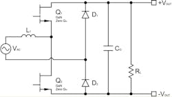
Most high-end power supplies in the range from 700W to 3000W and even higher strive to optimize efficiency, cost and power density. This is particularly true for datacenter applications. Most of these power supplies take advantage of GaN in the PFC section, by operating with a front-end consisting of a Bridgeless Totem Pole PFC (Fig. 1). This configuration achieves 28% lower power losses compared to traditional boost PFC circuits.
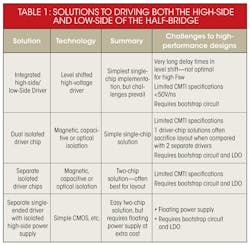
Most switching power supplies use multiple half-bridge circuits, often interleaved for higher power, to create not only the PFC circuit, but often the LLC and other topologies that almost exclusively rely on half-bridge and full bridge circuits. There are several general solutions to driving both the high-side and low-side of the half-bridge, as summarized in Table 1.
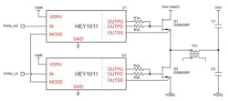
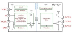
Heyday’s HEY1011 integrated solution, shown in Fig. 2, optimizes layout, provides isolation, is cost-effective, and requires no bootstrap circuit or floating power-supply circuit.
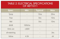
Used with GaN Systems’ GaN FETs, Heyday’s new line of 650V high-side GaN drivers do not require bootstrap diodes or capacitors and offer superior performance figures compared with other drivers. These drivers exhibit low propagation times of <25ns, and are capable of operating frequencies into the MHz range opening opportunities for systems designers to capture the capabilities of both ever-improving MOS devices and the best GaN devices available.
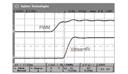
Restrictions to higher operating frequencies include the drivers and the bootstrap diode. The reverse recovery losses in the diode are a disabler at higher frequencies and start to become prohibitive even at 500 kHz and above. Heyday’s drivers do not need any bootstrap components, which enables more efficient drive even in the hundreds of kHz range and into the MHz range. Bootstrap components also suffer from some nasty negative performance anomalies such as bootstrap capacitor “overdrive.” This occurs when the bootstrap capacitor is charged above the intended drive voltage due to negative spikes on the converter switching node. This overcharging can cause the gate of the GaN device to operate outside its specified limits. Heyday’s technology completely alleviates this problem. Figure 3 shows the total propagation from PWM input from controller out to VDRIVE into a 1nF load capacitor of 18ns.
Heyday uses a fully integrated magnetic isolation-based transformer to transfer the gate drive signal and the gate drive energy (Fig. 4). So transferring the energy internally in the device importantly eliminates the need for the bootstrap components. These drivers are packaged in fully integrated surface-mount packages.
The dv/dt immunity figure of the Hey1011 GaN FET driver is >100V/ns. This enables robust fast switching systems, which is very important for GaN-based converters.
These drivers also allow for negative voltage swings on the switched reference node of the driver. For example, in the case of a half-bridge technology, if the center switched node swings negative, no problems occur for these drivers. The Hey1011 negative swing limit is as low as -650V.
The drivers also deliver bipolar outputs for securely driving the enhancement mode GaN devices into the off state. The Hey1013 delivers gate drive voltages of -2V to +6V.
The Hey1021 also can generate a gate-drive voltage of 4.5V to 6V amplitude, all from a single +3.3V ground referenced supply. From a single ground-referenced 3.3V supply, the Hey1011 generates a high-side 650V drive with a settable 4.5V to 6V amplitude.
Continuous “on” capability is also a useful feature of these drivers. Normally with bootstrap circuits, very long on-times are not possible, as the bootstrap capacitor needs to be topped up. But Heyday drivers have a built-in automatic refresh that can deliver a continuous “on” indefinitely. This can be very useful for automotive applications.
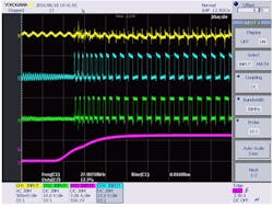
“First-pulse-perfect” is an inherent capability of the magnetic coupling technique, the first pulse being the same as all subsequent pulses. Figure 5 shows low- and high-side gate-drive pulses from the Hey1012 in a closed-loop LLC system (VIN = 400V, VOUT = 12V) with an ILOAD step from no-load to 6A. The first driver pulses follow the controller requested pulses perfectly, even after being “off” for a long duration.
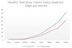
In static mode the guaranteed maximum quiescent current on all Heyday driver products is < 400uA. This is very useful for systems that require low standby or sleep-mode power consumption without the need for a sleep pin. Figure 6 shows the current consumption of the Hey1011 GaN driver versus frequency driving a 220pF/1nF load capacitor.
Heyday driver devices are sampling now and will be available in fully integrated surface-mount packages in December 2016. The drivers are 2kV, human-body-model ESD-compliant with die temperature capability of -40°C to 125°C.
