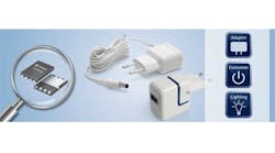
The need for slimmer, smaller chargers for mobile devices, HDTVs, and LED lighting led to the creation of the ThinPAK 5x6, a leadless, surface-mounted (SMD) package for CoolMOS MOSFETs. Developed by Infineon, the 1-mm-high, 5- by 6-mm-footprint ThinPAK 5x6s cut volume by 80% compared to traditional SMD packages like the DPAK. Low parasitics, such as lower source inductance versus the DPAK, reduce gate oscillation under all load conditions and minimize voltage overshoots during switching by 40% compared to traditional SMD packages, according to the company, improving device and system stability. Overall, the smaller ThinPak 5x6 adds flexibility to printed-circuit-board designs and boost switching performance, leading to more efficient power conversion while reducing system size in applications such as low-power adapters, lighting and thin-panel TVs.
Comments
